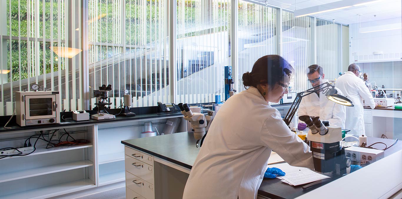
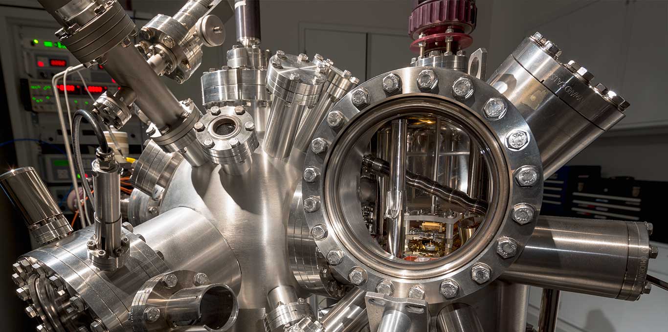
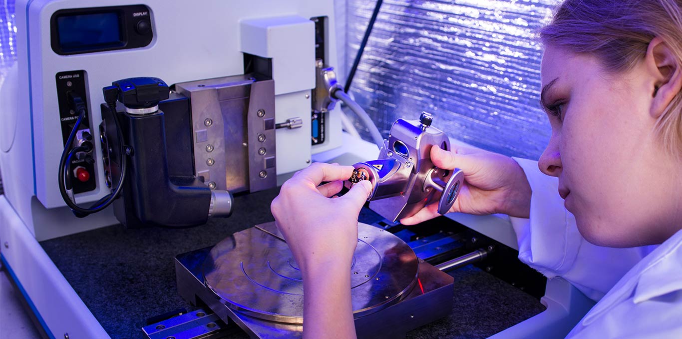
The Singh Center is a next-generation nanotechnology center that merges traditional approaches to nanoscale development with unique state-of-the-art equipment, materials, and ideas.
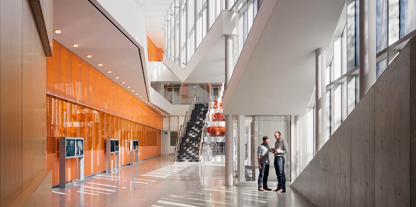
Working at the Singh Center
Experienced faculty and staff are committed to the success of the scientists and researchers using the facilities Meet the team