Xilinx ModelSim Simulation Tutorial
CSE 372 (Spring 2006): Digital Systems Organization and Design Lab
ModelSim is a tool that integrates with Xilinx ISE to provide simulation and testing. Two kinds of simulation are used for testing a design: functional simulation and timing simulation. Functional simulation is used to make sure that the logic of a design is correct. Timing simulation also takes into account the timing properties of the logic and the FPGA, so you can see how long signals take to propagate and make sure that your design will behave as expected when it is downloaded onto the FPGA.
Functional Simulation
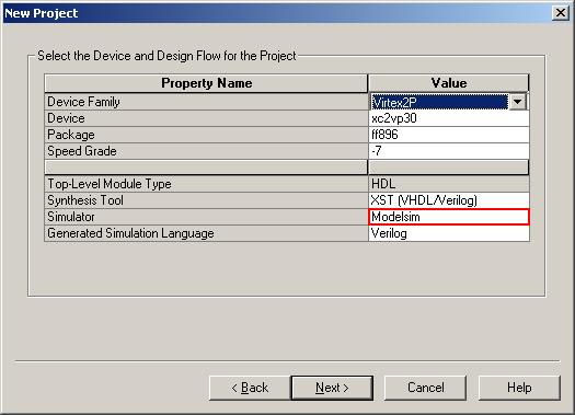
Open the ISE Project Navigator and create a new project. After entering a project name and location, you'll be prompted for the project properties. Set the properties as shown below, making sure to select Modelsim as your Simulator.
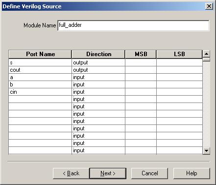
Click Next, and create a new Verilog Module source named full_adder. The inputs and outputs for the module are shown below. Once you've entered them, click Next and Finish until your module is generated.
Note
If you accidentally select ISE Simulator as the simulator for your project, or if you open a previous project that had the ISE Simulator selected, you can change the simulator by right-clicking on xc2vp30-7ff896 in the Sources in Project window and selecting Properties.
This tutorial will use a full adder that is the same as the one you created in Lab 0. You can use your own code, or copy the solution below:
module full_adder(s, cout, a, b, cin);
    output s, cout;
    input a, b, cin;

    wire t1, t2, t3;

    xor (t1, a, b);
    xor (s, t1, cin);
    and (t2, t1, cin);
    and (t3, a, b);
    or  (cout, t2, t3);
endmodule
Run the Check Syntax process (under Synthesize) to make sure your code is entered correctly, and save your design.
Right-click on full_adder.v in the Sources in Project window and choose New Source. Select Verilog Test Fixture and give your file a name such as "test_full_adder". Click Next, and you'll be prompted to associate the file with a module; choose full_adder, click Next, then click Finish. The file will be added to your project.
ISE creates a skeleton test fixture for you. The inputs to the module are registers ("reg") because they are assigned in a procedural block (the section between "begin" and "end"). The outputs from the module are wires. The full_adder module is instantiated and the simulation begins after the "initial begin" line. The values are initialized, and your code goes under the "Add stimulus here" line.
Simulate your module by assigning different values to the inputs and observing the outputs. Between assignments, delays are inserted using #n, where n is the number of nanoseconds of delay. For example, the following code tests when each of the inputs are high separately, changing the inputs every 25 ns:
// Add stimulus here
//125 ns
#25;    a = 1'b1;
//150 ns
#25;    a = 1'b0;   b = 1'b1;
//175 ns
#25;    b = 1'b0;   cin = 1'b1;
Note
For the value 1'b0, the 1 represents the number of bits, the b stands for binary and the 0 represents the 1-bit binary value. Values can also be represented in decimal and hexadecimal; for example, 8'd27 represents 00011011 and 4'hA represents 1010.
A good test fixture will test all or most of the possible inputs to the module, and especially any corner/boundary cases. Since the full adder only has three one-bit inputs, there are only eight possible input combinations, and your test fixture should simulate them all. Write the rest of the simulation code yourself; if you need help, you can view a completed test fixture here.
Once you have written and saved your test fixture, click on it in the Sources in Project window, then click on the Process View tab below. Expanding the ModelSim Simulator item reveals the possible simulation options. Double-click on Simulate Behavioral Model and ModelSim will open, compile your full adder module and run the simulation code.
The black and green section of ModelSim is the waveform area. To scale the waveform correctly, move the horizontal slider all the way to the beginning (the left), then click the Zoom-Out 2x button until a proper scale is reached. For this design, a suitable scale is from 0 ps to about 200000 ps (200 ns) or 400000 ps (400 ns).
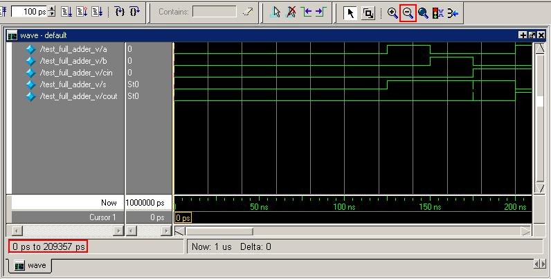
The leftmost column of the wave area lists the input and output signals for the test module, test_full_adder_v. These signals can be rearranged and deleted. The column to the right lists the values of the signals at the cursor. To set the default cursor, Cursor 1, click anywhere in the waveform. To move the cursor to the exact location where a signal changes, click on the signal so it is highlighted in white, then click the Find Previous Transition and Find Next Transition buttons (
 ) on the toolbar.
Note
Your output signals may have "false" transitions at times when more than one input signal changes. This is normal.

"False" transitions in two output signals.
The cursor can be locked by right-clicking on the time at the bottom of the cursor and choosing Lock Cursor 1. The cursor can be renamed by right-clicking on the white box in the lower-left. The time of the cursor can also be precisely set by right-clicking on the box to the right of the cursor name. You can create a new cursor by right-clicking at the bottom of the waveform and choosing New Cursor, or by using the Insert Cursor button on the toolbar. Cursors can be deleted in this way as well. If you have multiple cursors, the time between them is shown in white at the bottom of the waveform.
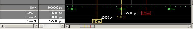
A waveform with three cursors. Cursor 1 is locked, so it cannot be moved accidentally.
You can visually check that your module functions correctly by observing which of the input signals are high and checking that the outputs are correct. It may be helpful to drag the cursor across the waveform, so you can look at the numerical values of the signals instead of looking at the waves themselves. For modules with vector signals (rather than single-bit signals), you can right-click on the signal values and change the radix to display the values in binary, decimal, hexadecimal, etc. The output values have an "St" in front of them because they are set to the Symbolic radix by default; change this to Binary or another format.
Warning
Use the Unsigned radix, rather than the Decimal radix, to view signals as decimal values. Signed decimal values can cause confusion.
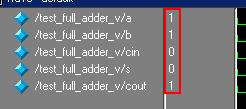
Drag the cursor across the waveform to see these values change, and check that the outputs are correct for the given inputs.
Close ModelSim when you are finished. If you make changes to your module in ISE, the easiest way to restart the simulation is to close ModelSim, then run the Simulate Behavioral Model process again.
Note
The ModelSim license only allows one instance of ModelSim to run on a computer at any time.
Advanced Functional Simulation
Instead of visually checking your simulation outputs every time you run the simulation, you can write test code that will check the outputs for you. For each output, you can write a task that takes an input value and checks that it matches the current output. If it does not, it will print an error to the simulation console. The code for the tasks for s and cout is below:
task CHECK_s;
    input NEXT_s;
    #0 begin
        if (NEXT_s !== s) begin
            $display("Error at time=%dns s=%b, expected=%b", $time, s, NEXT_s);
            end
        end
    endtask
task CHECK_cout;
    input NEXT_cout;
    #0 begin
        if (NEXT_cout !== cout) begin
            $display("Error at time=%dns cout=%b, expected=%b", $time, cout, NEXT_cout);
            end
        end
    endtask
The code for these tasks goes in your test fixture file, below the simulation block (from "initial begin" to "end"). These tasks are "called" in the simulation block at an interval after the inputs have been assigned, to allow time for the signals to propagate. For example, the first two cases are below:
// Add stimulus here
//125 ns
#25;    a = 1'b1;
//150 ns
#25;    CHECK_s(1'b1);  CHECK_cout(1'b0);
//175 ns
#25;    a = 1'b0;   b = 1'b1;
//200 ns
#25;    CHECK_s(1'b1);  CHECK_cout(1'b0);
For a complete test fixture file that uses these tasks, click this link. If your simulation has any errors, the time of the error, the current output and the expected output will be displayed in blue in the ModelSim console (the "Transcript" window). If your simulation has no errors, nothing will appear.
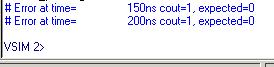
Simulation errors displayed in the ModelSim console.
Hint
If your simulation has errors, you can go back, fix your module and re-use the same test fixture to test the module again. It is a good idea to create a complete and accurate test fixture to begin with, so it can continually be used to test your module.
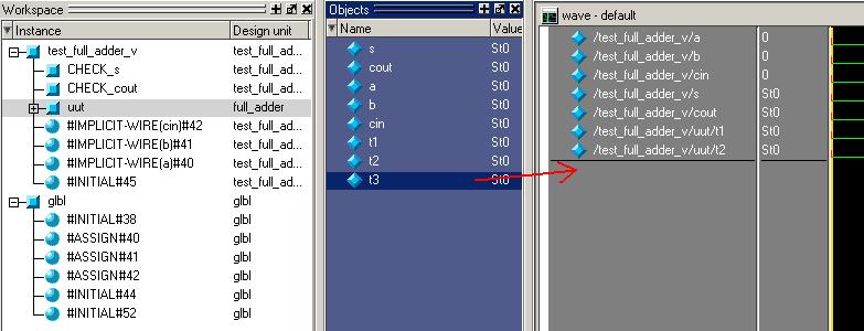
In some designs, you will want to observe internal signals that are not inputs to or outputs from the module. In the full adder, we can observe the intermediate internal wires t1, t2 and t3. Click on uut in the Workspace window (on the left side of the ModelSim window). All of the wires in the uut module (unit under test, or the full_adder module) appear in the Objects window. Drag t1, t2 and t3 to the signals section of the waveform to add them.
Hint
Make sure you drag the signals from the Objects window. Dragging signals from the Workspace window will not work properly.
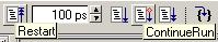
Immediately after adding the signals, they will not have any waveforms, and will have a value of "No Data" if you move the cursor. In order to read these signals, ModelSim must run the simulation again. To do this, first click on the Restart button on the toolbar, leave all of the boxes checked on the subsequent prompt and click Restart. ModelSim will reload the simulation, but will not re-run it; click the ContinueRun button on the toolbar to start the simulation again. Waveforms will now appear for t1, t2 and t3.
Note
Restarting and running the simulation again will not incorporate any changes you have made to your module or test fixture. To see the effects of these changes, close ModelSim and run the Simulate Behavioral Model process again in ISE.
Note
The ContinueRun button will run the simulation for as long as 1000 ns (1 us). If you need your simulation to run for longer, enter a value in the Run Length box (i.e. 10000 ns) and click the Run button to the right of it.
Timing Simulation: Combinational Logic
In order to perform a full timing simulation, ISE must first synthesize, translate, map, and place & route your design. To start the timing simulation, click on your test fixture file and run the Simulate Post-Place & Route Verilog Model process. If you have not already run the synthesization and implementation processes, they will be run automatically (this may take several minutes), and ModelSim will open.
The waveform for the timing simulation will look slightly different than the one for the functional simulation. An additional signal, GSR, will be added. GSR is a global reset signal and is high for the first 100 ns. You will also notice that the output signals are red and have a value of "x" at the beginning of the simulation. x means the value of the signals is unknown; this is because the inputs have just been initialized, and the signals have not propagated through the module to the outputs.
Scroll to the first transition of signal a and look at signal s: instead of changing at the same time as signal a, like it did in the functional simulation, the signal transitions after a delay. Using two cursors, the delay is measured to be 3983 ps, or 3.983 ns.
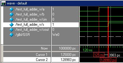
Go back to the ISE Project Navigator, select your full_adder.v file (the module, not the test fixture) and double-click on the View Design Summary process. Under the Detailed Reports section, click on Post Place and Route Static Timing Report. Under the Pad to Pad section, the delay from signal a to signal s is listed as 3.983 ns, which matches what we found in our timing simulation.
Another important timing measurement can be found in the synthesis report; view it by expanding the Synthesize process and double-clicking on View Synthesis Report. Scroll down to the Timing Summary section, and you will see Maximum combinational path delay: 4.591 ns. This is the maximum delay for signal propagation in your design, so changing signals faster than this will result in unexpected behavior.
To see an example of this, go back to your test fixture and change every instance of "#25" to "#1"; this means that the signals will change every two nanoseconds (with check tasks in between), as opposed to every fifty nanoseconds. Run the timing simulation again and you will see incorrect waveforms (and errors in the console, if you are using check tasks).
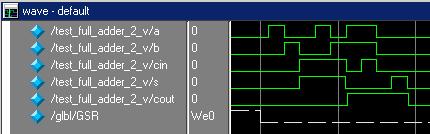
A timing simulation with transitions every 2 ns. The output signals do not match the input signals because the inputs change too quickly.
Timing Simulation: Sequential Logic
Some changes must be made to the test fixture in order to simulate a clocked design. Here is a sample clocked design, a two-bit up/down counter, written in behavioral Verilog. Add the file to your project and add a new test fixture for the module. In your test fixture, instead of manually changing the clock, some behavioral Verilog code can change it for you. Put this code outside of the initial block:
always #5 CLK <= ~CLK;
This will make CLK transition every 5 ns, giving a clock period of 10 ns, or a clock frequency of 100 MHz. The only other input to change is IN, which is done as usual under the Add stimulus here comment. Run the Simulate Behavioral Model process to simulate the module in ModelSim. Change the radix for OUT to Unsigned to easily see the counter count up when IN is low and down when IN is high.
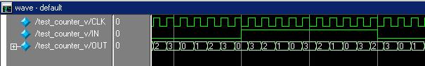
A functional simulation of a clocked counter module. The clock period is 10 ns.
Run a timing simulation on the module by executing the Simulate Post-Place & Route Verilog Model. The counter changes on positive clock edges, so the time from a CLK transition from low to high to the change in OUT is the propagation delay. Zoom in closely on an OUT transition, and you should notice that on every other cycle, OUT changes to one value, then quickly changes to another value (the expected value). If you expand OUT, you can see that the two OUT bits do not change at the same time. This is not a problem for our current design, because everything changes before the next positive CLK edge. However, if the positive CLK edge fell between the OUT[0] and OUT[1] transitions, unexpected behavior would arise. This is why it is important to use timing simulation in addition to functional simulation.
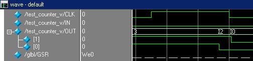
A timing simulation of the clocked counter module. The measured propagation delays should match those in the Post Place and Route Static Timing Report.
Open the Synthesis Report and find the Timing Summary section. There should be a line saying Minimum period: 1.348ns (Maximum Frequency: 741.867MHz). Using a clock period of less that 1.348 ns will create unexpected behavior.
References
Designing and Testing an Adder
Verilog HDL On-Line Quick Reference
Authors: Peter Hornyack, Milo Martin