Lab 2 - Non-Pipelined Processor
CSE 372 (Spring 2007): Digital Systems Organization and Design Lab
Worksheet due Friday, March 2nd
Demo by Tuesday, March 20th
Writeup due before class on Friday, March 23rd
This lab is to be done in groups.
This lab is worth 25 points.
Overview
In this lab, you'll combine your ALU from lab1 with a register file, controller, branch logic, and other datapath elements to create a non-pipelined P37X processor.
Note
The final lab of the semester, lab3, is substantially more time consuming than this lab. Thus, even though you have a few weeks to complete this lab, your goal should be to complete it quickly such that you have plenty of time for the next lab.
Common Module Library
Register Module
As discussed in class, we're giving you the Verilog code for a multi-bit flip-flop register. Please use this single register module unmodified in your design. This register should be the only state element you use anywhere in your design (aside from the main memory module we're also giving you):
module Nbit_reg(in, out, clk, we, gwe, rst);
   parameter n = 1;
   parameter r = 0;

   output [n-1:0] out;
   input [n-1:0]  in;
   input          clk;
   input          we;
   input          gwe;
   input          rst;

   reg [n-1:0] state;

   assign #(1) out = state;

   always @(posedge clk)
     begin
       if (rst)
         state = r;
       else if (we & gwe)
         state = in;
     end
endmodule
This register module has several features:
- A "write enable" (we) signal to control when the register is written.
- A parameterized bit width (n, the first parameter of the module).
- A parameterized reset value (r, the second parameter of the module), allowing the initial value of a register to be any value.
- A "global write enable" (gwe) signal to enable the single-stepping described in the tutorial. Just as clk and rst are passed into your modules unmodified, you should do the same with gwe as well.
- A 1-unit delay on the register outputs to ensure the functional simulation works correctly.
Note
The above code is included in the p37x_processor_skeleton.zip archive in he file register.v. We suggest you use this register to avoid duplication of code.
Multiplexors
Create a set of parameterized muxes to instantiate explicit structural muxes in the datapath. You'll need N-bit muxes that are 2-to-1 (datapath), 4-to-1 (datapath), and 8-to-1 (in the register file).
For example:
module mux_4to1_N(out, sel, a, b, c, d);
   parameter n = 1;

   output [n-1:0] out;
   input [n-1:0]  a, b, c, d;
   input [1:0]    sel;

   assign         out = sel == 2'b00 ? a :
                        sel == 2'b01 ? b :
                        sel == 2'b10 ? c :
                        sel == 2'b11 ? d : {{n}{1'b0}} /*unused*/;
endmodule
Note
A few multiplexors are included in the p37x_processor_skeleton.zip archive in the file mux.v. We suggest you use these muxes to avoid duplication of code.
3-to-8 Decoder
To build the register file, you'll need a 3-to-8 decoder. A 3-to-8 decoder has a single 3-bit input and a single 8-bit output. Recall that exactly one of outputs of a decoder is one; the rest will be zero. If the 3-bit input value is n, then the nth is the bit set to one. As with the multiplexors, the use of the nested conditional operator should make this structure relatively easy to specify in Verilog.
Register File
Register File Interface
The P37X ISA uses eight registers and follows a two-input, one-output operation format. As such, the register file should have eight registers accessed via two read ports and one write port. Your register file module regfile8_16_2r1w should have the following interface:
- Two 3-bit input register read select signals: rsel1 and rsel2.
- One 3-bit input register write select signal: wsel.
- Two 16-bit output register read data signals: rdata1 and rdata2.
- One 16-bit input register write data signals: wdata.
- One 1-bit input register write enable signal for the single write port: wen.
- One 1-bit input global write enable signal: gwe.
- One 1-bit input reset signal: rst.
- One 1-bit input clock signal: clk.
In a given cycle, any two registers may be read and any register may be written. A register write occurs only when the wen signal is high. If the same register is read and written in the same cycle, the old value will be read (not the new value being written).
Register File Implementation
Create a register file module with the interface specified above. Before you write the Verilog code for the register file, first draw a diagram of the circuit with all wires and input/outputs labeled. Include this hand-drawn schematic with your lab writeup.
Implement the register file as described in the CSE371 lecture notes on datapath design. Use the n-bit register described above to implement the register storage. Each read port uses a 16-bit 8-to-1 multiplexor to select the outputs of one of the eight 16-bit registers. The write port uses the output of a 3-to-8 decoder combined with the write enable input to drive the write enable on the individual register's write enable signals. In all, you'll instantiate eight registers, one decoder, and two multiplexors and then connect them as needed.
Note
Although the CSE371 notes may occasionally talk about using tri-state devices for fast multiplexors, we're not going to use tri-state devices. When used incorrectly, tri-state devices can cause lots of problems. In addition, Xilinx should detect the multiplexors modules and generate its own fast multiplexors (assuming your Verilog code is clean enough).
Register File Testing
To encourage you to perform bottom-up testing of your design, we're giving you a testbench for testing just the register file component: regfile_testbench.v and regfile.input.test
You should verify that your design fully synthesizes without error and works correctly in ModelSim.
The Datapath
As described in class, the non-pipelined datapath (the link points to a .pdf file of the datapath) contains the register file, memory, PC register, branch logic, 11 muxes and 2 write enable signals:
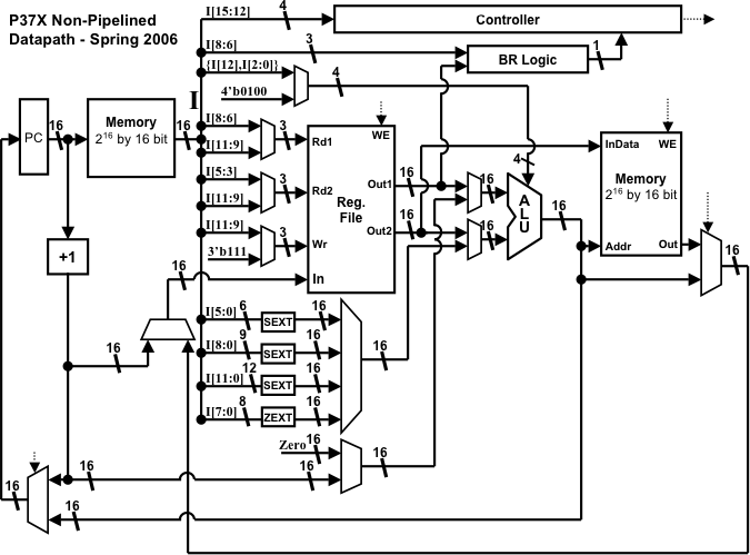
In our implementation, the main datapath module was approximately 150 lines of Verilog.
Arithmetic/Logical Unit (ALU)
The ALU from lab1 is a key components of the processor. You can use your ALU unmodified, or you can optionally use the faster built-in + and * operators.
Branch Logic
The branch unit determines if a conditional branch should be taken or not-taken. It has two inputs: (1) a 16-bit signed value and (2) a three-bit "NZP" condition from the instruction (negative, zero, positive). The only output is a one-bit signal: 1 for taken branch, zero for not-taken (fall-through) branch. For example, if the N/Z/P bits are 110 and the data input value is negative or zero, then the output will be a one.
Internally, you'll want to create logic to determine if the 16-bit input value is (a) zero, (b) negative, or (c) positive (of which at most one will be true). This three-bit NZP value combined with the three-bit NZP bits from the instruction to generate the one-bit output. This branch logic can actually be encoded in just a few lines of Verilog. We suggest that you first determine if the input value is negative (hint: you can just look at a single bit of the value), zero (hint: use the reduction operator "|"), and positive (hint: a number is positive if it is not negative and not zero).
Note
You can use Verilog's == operator, but the < and > operators in Verilog assume that multi-bit values are unsigned, and thus won't work correctly on the signed input value.
Controller
The controller has two inputs: the 4-bit opcode and the 1-bit branch outcome from the branch logic. The outputs of the controller are all of the control signals for the 11 muxes and 2 write enable signals.
We suggest you write the Verilog for this module in two parts. The first part should decode all of the opcodes, one per line:
wire is_STR           = (opcode == 4'b1101);
...
wire is_ST            = (opcode == 4'b1111);
The second part can determine the actual output signals using these decoded values:
assign mem_we = (is_STR | is_ST);
Using this basic format, the controller module body should be much less than 100 lines of Verilog.
Program Counter
The program counter is just a 16-bit register. The initial value of this register should be 512 (hex 0x0200), which is the first memory location after the trap and interrupt tables. This initial value can be set via the reset parameter of the register module.
Multiplexors
Use the multiplexor modules described above to explicitly instantiate the structural multiplexors. Recall that sign extension and zero extension can be done easily in Verilog using the "repeat signal" and "concatenate signal" operators (as discussed in class). This sign exertion can be performed as an input value to a multiplexor, reducing the number of lines of Verilog code and avoiding intermediate wire names.
System Interface and Memory
The top-level processor (which is available as p37x_processor_skeleton.zip), instantiates the memory module, the processor module, all of the device code, generates the clock, etc. As such, the "memory" is not actually instantiated inside the datapath module. Instead, all of the memory module signals are inputs/outputs to the datapath module:
module sc_datapath(CLK, RST, GLOBAL_WE,
                   IMEM_ADDR, IMEM_OUT,
                   DMEM_ADDR, DMEM_IN, DMEM_OUT, DMEM_WE,
                   REGFILE_WE, REGFILE_DATA_IN);

  input         CLK;         // main clock
  input         RST;         // global reset
  input         GLOBAL_WE;   // global we for single-step clock

  input [15:0]  IMEM_OUT;    // output from insn. memory
  input [15:0]  DMEM_OUT;    // output from data memory
  output [15:0] IMEM_ADDR;   // insn. memory address (i.e., current PC)
  output        DMEM_WE;     // data memory write-enable
  output [15:0] DMEM_ADDR;   // data memory address
  output [15:0] DMEM_IN;     // input to data memory

  output        REGFILE_WE;        // testbench/debugging signal
  output [15:0] REGFILE_DATA_IN;   // testbench/debugging signal

  ...
The last two output signals (REGFILE_WE and REGFILE_DATA_IN) are exported to allow the testbench to check for correct behavior and for supporting the debug mode.
Testing
As we did with previous labs, you'll use a behavioral testbench to test your processor. See a tutorial on the testbench.
You will also test your processor on hardware. See this hardware tutorial to do this.
Verilog Restrictions
This lab should be implemented using only low-level structural Verilog and the assign statement. However, in this lab, you are allowed to use the additional Verilog operators: +, -, *, /, <<, >>,. However, as before, you shouldn't use any of the behavioral Verilog constructs. If you're not sure if you're allowed to use a certain Verilog construct, just ask (post a message on the newsgroup, send an e-mail, etc.).
Demos
You'll have to demonstrate that your design works using both simulation and the hardware prototyping boards:
- Simulation: Using the testbench code for this lab, demonstrate that your processor works correctly in functional simulation. You'll be asked a bit about your code (all group members) and given some additional test inputs to simulate.
- Hardware: Using the memory system with devices (see the hardware tutorial for these and other necessary files), you'll demonstrate that your design works correctly on your board using the test hex file we give you.
What to Turn In
Worksheet: Turn in the complete datapath worksheet by the due date listed above.
Final Writeup: You'll turn in the final writeup in class:
- Verilog code. As before, your Verilog code should be well-formatted, easy to understand, and include comments where appropriate (for example, use comments to describe all the inputs and outputs to your Verilog modules). Some part of the project grade will be dependent on the style and readability of your Verilog, including formatting, comments, good signal names, and proper use of hierarchy.
- In addition, answer the following questions:
- Once you had the design working in simulation, did you encounter any problems getting it to run on the FPGA boards? If so, what problems did you encounter?
- What other problems, if any, did you encounter while doing this lab?
- How many hours did it take you to complete this assignment?
- On a scale of 1 (least) to 5 (most), how difficult was this assignment?
Addendum
- [None, yet]