A successful DRC ensures that the layout passes through the rules designed
for faultless fabrication. However, it does not guarantee if it really represents
the circuit you desire to fabricate. In our case, for an inverter, we really
need a tool than can compare the connectivities of our layout with that of the
schematic and ensure that it is really a layout for an inverter. One way
Cadence does this is by generating an Hspice netlist file from the layout and
comparing it with the netlist for the schematic. This is the essence of
the LVS tool.
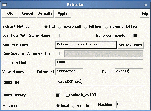
1. The first step is to extract all the connectivities and parasitic capacitances from your layout design. From the layout view window, choose Extract... under the Verify menu. A window will pop-up. Make sure that the entries are as given below. For the entry in Switch Names, click on Set Switches. A window will pop-up. Choose the option for Extract_parasitic_caps. Note that, if for some reason, you did not want to extract the parasitic capacitances, you would leave the Switch Names empty. Finally, click on OK. The beauty of this extraction tool is that Cadence will recognize not only all the connections but also more importantly, if you have designed the layout correctly, it will also recognize all the nmos and pmos transistors.
Make sure that your layout window is in Edit mode.
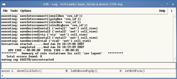
2. Your layout will then be extracted and while Cadence is doing so, the intermediary steps will be displayed in the CIW. It will tell you whether the extraction is successful or not.
3.a. Open the extracted view of the cell in edit mode from the Library Manager window. The extracted view will look something like this:
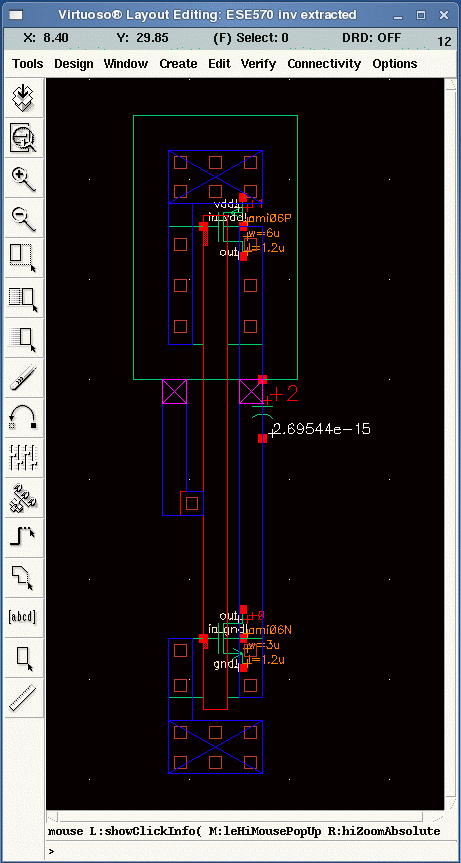
Just for fun, if you zoom into those small (really small) rectangles in the poly area of the above figure, you will see either “nmos4” or “pmos4” written on it. This shows that the Cadence has recognized that particular portion of the layout to be transistors. Press Shift-F to see the symbols for the active and passive devices appear in the extraction view window. This is just symbolic to associate the portions of the layout with different devices. It does not bear any connectivity information.
The next step is to perform LVS. Since we generated a layout with certain a
W and L for the transistors (for the case discussed here, the author had nmos W
= 3u and L = 1.2u and pmos with W = 6u and L = 1.2u), the layout versus
schematic operation (discussed below) will give you an error if the schematic
against which the layout is compared has a different W and L for its pmos and
nmos transistors. So, make sure that the nmos and pmos have correct entries in
their properties field for W and L.
3.b. Before you are about to perform LVS, you need to make sure that Cadence is checking for certain LVS rules. To do so, click on NCSU -> Modify LVS Rules … from the layout view window of your inverter. A window should pop-up with a number of LVS options available for you to choose. For our purposes, you should verify that the following 4 items are selected:
Allow FET Series Permutations, Combine Parallel FETs, Combine Parallel Capacitors, Compare FET Parameters
This check should be performed every time you are about to start an LVS.
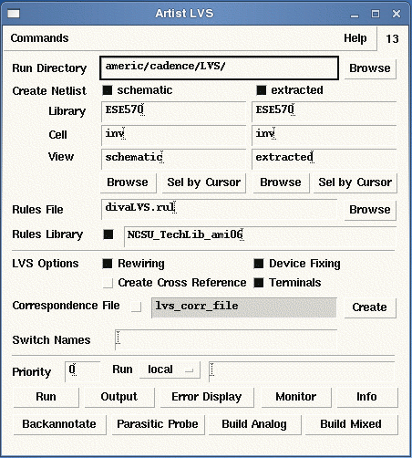
3.c. From the extracted window, choose LVS... under the Verify menu. A pop-up menu will appear. Type in the Run Directory that you want to run the LVS in, as well as the cell names that you want to run LVS on and all the other fields as shown in the inverter example below. It is advisable to put the run directory in the /tmp/username as you might run out of disk quota when designing huge layouts. If you already had an LVS directory, a window will pop-up which might say " The selected LVS rule directory does not match the run form". Just select Form Contents and click OK.
Click on the Run button and wait.
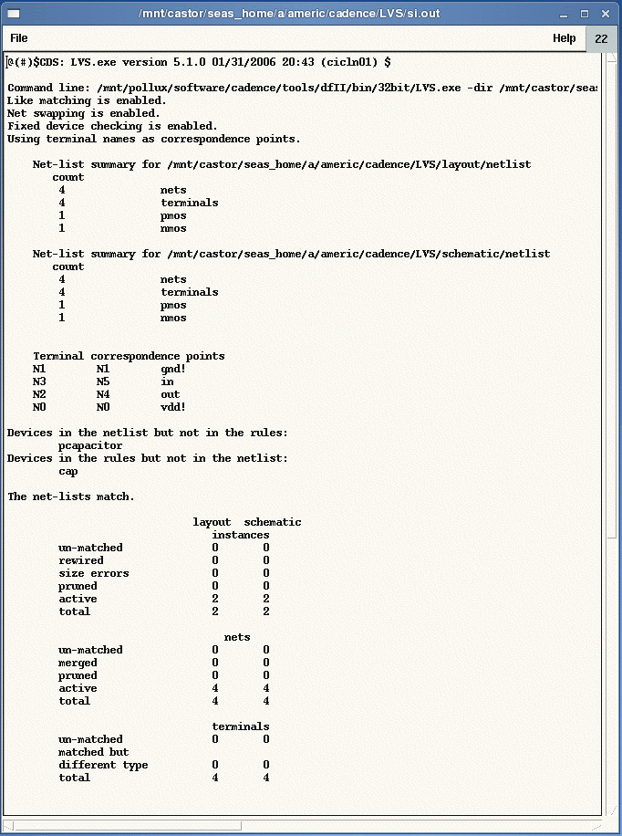
Select the particular LVS job that is currently running and click from the menu Command -> Show Run Log. The si.log output file will pop-up as shown below.
5. A pop-up menu will then appear notifying you of the successful completion or failure of the LVS job.
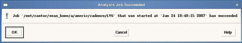
Click on the OK button.
6. We see from the si.log file above that there are no errors in the LVS comparison. However, there could have been errors if, for example, the W and L values of the transistors in the schematic window did not match with the W and L values of the transistors in the layout. If there are any errors, click on Error Display in the LVS menu to view what went wrong. It is very beneficial if you click on Help in the si.log output window shown above. It will explain each of the terms in the above window in great detail. The si.log will also explain to you all the errors that it detected in both the schematic and layout views during the LVS comparison.
The following points illustrate a situation if we had an error in the previous step.
7. By clicking on Error Display in the LVS window, the LVS Error Display window will pop-up. Select or deselect the various options so that the errors that will be shown are only those that you want to see at this point. In our case, the only errors we encounter is the size errors and to see that, we select parameters under the Unmatched field.
8. To zoom into each error, select the Auto-Zoom option and then click on the First button from the Display buttons. To view each error in sequence, keep clicking on the Next button. You will see each error being highlighted by whatever color you selected from the Error Color menu in the extracted window. The default color should be “hilite.d1”. You should pick a color that is easy for you to see in the extracted view.
9. To get more information about the error, click on the Explain button. Then move your cursor above the highlighted point/area and click on the left mouse button. A pop-up menu will appear. Sometimes the information given is not very helpful. This is where your problem-solving skills come to play and are being sharpened.
10. Modify the layout or schematic appropriately and rerun the LVS check till your layout design is perfectly matched to the schematic view.
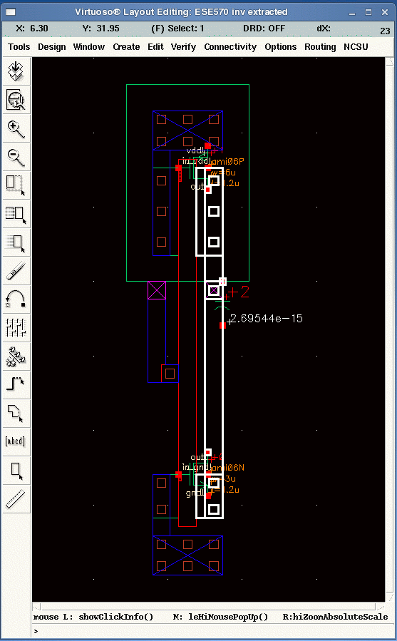
11. There is also a feature that can help you in debugging the layout; especially in checking the connections of your nets. Move your cursor to the net you want to highlight and click on the left mouse button. Anything that is connected to that net will be highlighted in white. You are then able to determine which connection or connections should not have been made to that net based on what has been highlighted. An example of the highlight is shown below.
One should realize that almost no one designs a perfect layout on the first attempt so do not expect to pass the LVS check on your first try. In most cases, there will be many errors reported by both the si.log file and the Error Display window. You should not be intimidated by all these errors. Many of these are, in fact, related to each other. Hence, once you fix one of these errors, many of the other errors should disappear. The idea is to concentrate on one error at a time, change the layout design accordingly and repeat the extraction and LVS steps until the layout and schematic views match perfectly with each other.
 |
 |
|
| previous | top | next |