Elionix Recipes
Updated on 9/30/2014
Contents
1 Basic Idea of Lithography CAD Program of ELS-7500EX system
1.1 Pattern Design on "WecaS" program
1.2 Pattern Design on GDS II or dxf CAD program
1.3 Condition File
1.4 Multiple Chip Placement
2 Setting up Exposure Conditions
2.1 Exposure Conditions
2.1.1 Resist Thickness
2.1.2 Resist Sensitivity
2.2 Beam Current Setting
2.3 Personal Setting
2.4 Dose Calculation
3 Exposure Recipes
4 Alignment Mark Preparation
5 Alignments of the same multiple patterns with the same registration marks
6 SEM and EXP mode
1. Basic Idea of Lithography CAD Program of ELS-7500EX system
Note:
- If you draw the design on "WecaS" program in the ELS-7500 EX system directly, you have to spend a time to draw the design on Elionix. We recommend you to draw the design independently, using "WecaS" or GDS II CAD program on the stand alone computer next to Elionix e-beam writer. You can also use the dxf file on "WecaS" program. Here, GDS and DXF CAD programs are commonly used.
- "Chip" (an exposure field without moving the stage) size determination guidelines based on minimum pattern line width
- For line widths of 20nm or less, 75um chip
- For line widths of 20nm or more, 150um chip
- For line widths of 50nm or more, 300um chip
- For line widths of 150nm or more, 600um chip
1.1 Pattern Design on "WecaS" program
you are going to
- set up the pixels [dots] and size [μm] of Chip
- place the Chip(s) at the location(s) desired
- create the pattern in the Chip area, using the CAD functions of "WecaS" program on the stand alone computer
- save the information on the pattern and Chip on the computer in the ELS-7500 EX system.
- See the following training manual: 75EXECATrainingManual_No1
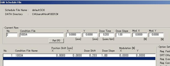
- Tip: The coordinate system on WecaS CAD program corresponds to the coordinate system on the stage. In other words, if you draw the pattern at (10 mm, 10 mm) on WecaS CAD program (global coordinate), as shown in the training manual, and if you set the X and Y locations to be (0 mm, 0 mm) in the "Edit Schedule File" window (local coordinate), as shown below, then the exposure starts at (10 mm, 10 mm) point on the stage, although the center of the 10mm x 10 mm sample is placed at (86.8 mm, 83.0 mm) on the stage.
To avoid the trouble, you have the following two choices in the above case:
- If you draw the pattern at (10.0 mm, 10.0 mm) on WecaS CAD program, then the pattern needs to be moved to (86.8 mm, 83.0 mm) point. In order to do it, change the X and Y locations in the "Edit Schedule File" window from (0 mm, 0 mm) to (76.8 mm, 73.0 mm) in the above case because the global coordinate (10 mm, 10 mm) corresponds to the local coordinate (0 mm, 0 mm).
- If you draw the pattern at (86.8 mm, 83.0 mm) on WecaS CAD program, then the X and Y locations in the "Edit Schedule File" window should be (0 mm, 0 mm) because the global coordinate (86.8 mm, 83.0 mm) corresponds to the local coordinate (0 mm, 0 mm).
1.2 Pattern Design on GDS II or dxf CAD program
you are going to
- create the pattern independently, using GDS II or dxf CAD program
- save the gds or dxf file on the computer in the ELS-7500 EX system
- set up the pixels [dots] and size [μm] of Chip
- convert the gds or dxf file into the "Cell" file on "WecaS" program
- place the "Cell" file at the location desired
- place the Chip(s) at the location(s) desired
- save the information on the pattern and Chip on the computer.
1.3 Condition File
The information on the pattern and Chip is saved in CO6, CB6, and CC6 files created on the computer.
- CO6 file: This file used as a master exposure file is an ASCII command file created as *.CO6. This file contains exposure conditions for each chip. More specifically, it contains Chip Dose variables, chip positions (in units of mm), and the file names of the figures to be exposed on the respective chips. The chip names are handed down to the CB6 and CC6 files.
- CB6 and CC6 files: These files (*.cb6 or *.cc6) are for figures. The CB6 file is a binary file for the lithography hardware, and the CC6 file is an ASCII file for displaying figures on the CRT display and debugging.
- In principle, CB6 and CC6 files are not used as individual files. The CO6 file is responsible for controlling them, and the user usually has to take care of the CO6 file only.
- In fact, however, they can be called and displayed on the CRT screen for practical purposes.
- The figure coordinates in the CB6 and CC6 files are based on the chip dot coordinate system.
- Both CB6 and CC6 files define figures placed on a chip and the chip may be placed anywhere on the stage. That’s why the figures are expressed with chip dot coordinates that are taken as relative coordinates.
1.4 Multiple Chip Placement
- If the pattern size is more than the Chip size (field size), multiple chips must be placed. In this case, since the stage is moved from one Chip to another, stitching error may be considered.
- See the following training manual of dxf file conversion and multiple chip placement: 75EXECATrainingManual_No2
2. Setting up Exposure Conditions
2.1 Exposure Conditions
The following tips would help to draw finer patterns in a short time:
For finer patterns
- Resist Thickness: Thin
- Acceleration voltage: High
- Beam current: Small
- Beam diameter: Small
- Exposure field: Small
For shorter exposure time
- Resist sensitivity:High
- Beam current: Large
- Beam overlapping: Small
- Exposure field: Large
- Note: In WNF, acceleration voltage of 50 kV (maximum) is used only.
- See actual exposure recipes below.
2.1.1 Resist Thickness
Aspect ratio of the pattern width on the resist thickness: Less than 5
- For example, if the pattern is 100 nm line and space, then 300 nm resist thickness is reasonable.
2.1.2 Resist Sensitivity
Resist sensitivity depends on the condition.
2.2 Beam Current Setting
A) The following beam currents are available in ELS-7500EX system with different Objective Lens Aperture in the "Beam Memory" dialog box.
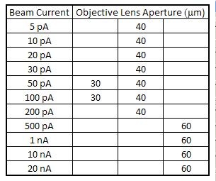
- Use the small aperture (30 μm) when a uniform beam diameter is needed over the entire exposure field.
- Use the medium aperture (40 μm) when using the smallest beam diameter over a relatively small exposure field.
- Use the large aperture (60 μm) when using a large beam current over a relatively small exposure field.
B) The following beam current can be estimated when it is assumed that the resist sensitivities of ZEP520A and PMMA are 60 and 500 μC/cm2, respectively, and that the dose time is 1 μsec/dot:
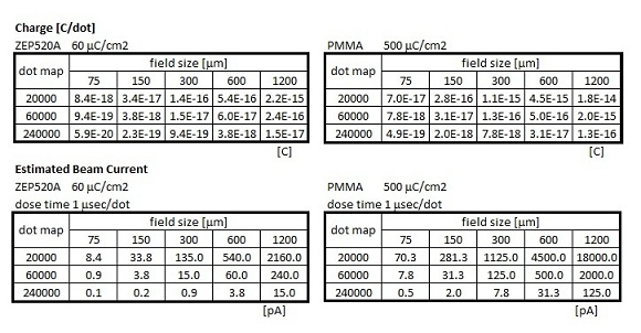
- The estimated beam current is reference only. Please see below.
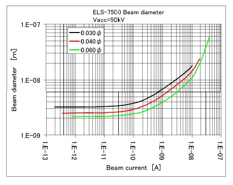
C) The beam diameter, which affects the minimum feature size, also depends on the beam current, as shown below.
- If I = 10 pA, then the beam diameter = 2-3 nm. If I = 10 nA, then the beam diameter = 10-20 nm.
2.3 Personal Setting
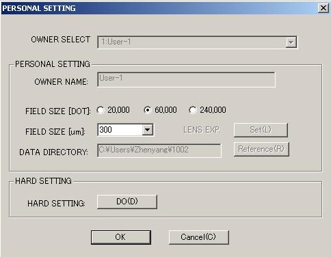
To estimate the position resolution, the exposure field has to be divided into some number of pixels (dot) depending on the field size. For example, to achieve the 10 nm position resolution, if the exposure field is 600 μm x 600 μm, then the field needs to be divided into 60,000 pixel x 60,000 pixel at least (600 μm /10 nm = 60,000). However, if the number exceeds 60,000, the exposure will be extremely time-consuming. On the other hand, if the exposure field is 75 μm x 75 μm, then the field needs to be divided into 7,500 pixel x 7,500 pixel at least (75 μm /10 nm = 7,500). Accordingly, we have to choose the appropriate dot map to achieve a desired position resolution, and to save the exposure time.
- This requirement does not always guarantee the minimum feature size because of proximity effect and electron-beam scattering at the resist and the substrate.
- In addition, in ELS-7500EX system, the beam diameter at the field center (2 nm) is unfocused at the field edge (50 nm at the 600 μm exposure field and 200 nm at the 1200 μm exposure field).
- If the pattern size is 300-600 μm, and the 10-30 nm minimum feature size is required, then the small beam current and the multiple chip placement with the exposure field (chip) size of 75 μm are recommended.
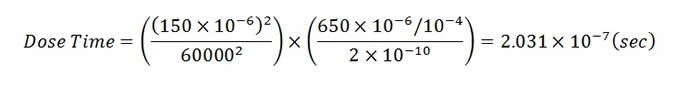
2.4 Dose Calculation
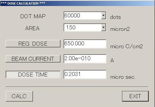
Dose time can be calculated using the following equation:
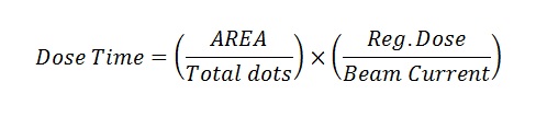
- Total dots: (DOT MAP)^2
- Area: The Dose Calculation dialog box shows the field size, but not the total area.
- AREA in the above equation is (Field Size)^2.
- In the above example in SI units,
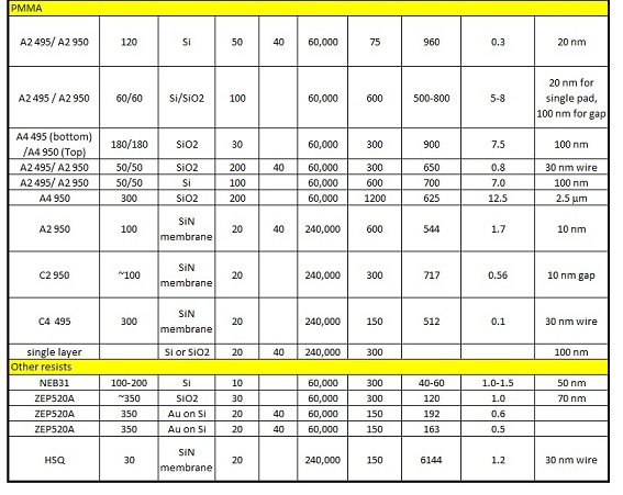
3. Exposure Recipes
The following exposure data is based on on-site inspections by Elionix and recipes of the users (updated on 12/5/2012).
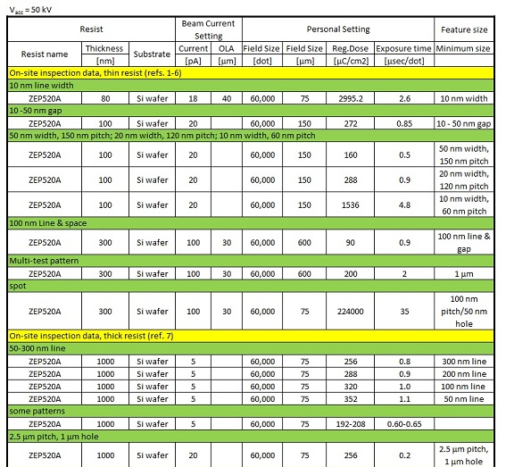
References
- UPenn_Inspection1
- UPenn_Inspection2_MultiTest
- UPenn_Inspection3_StitchingOverlay
- UPenn_Inspection4_CPGSpot
- UPenn_Inspection5_VariableField
- 080121OnsiteInspection_Fine
- 080121OnsiteInspection_Thick
4. Alignment Mark Preparation
1. Alignment marks can be made in the following two methods:
- ~1 μm depth etching into the substrate
- Lift-off of 20-100 nm thick metal
- Au, Pt, or W metals will work the best.
2. Alignment marks should be made on the 1st layer, so that the E-beam writer can adjust the location of the higher layer structure to align it with the 1st layer one.
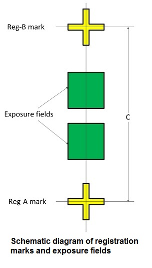
4.1 Reg-A and Reg-B marks
- In Elionix ELS-7500EX E-beam writer, rotational and positional misalignment corrections are carried out using a pair of marks, which are hereafter referred to as Reg-A and Reg-B marks.
- A schematic diagram of Reg-A and Reg-B marks and exposure fields is shown in the following:
- The distance C between Reg-A and -B marks should be more than 3.0 mm.
- There are no requirements for the shape of manual registration marks.
- The typical example of the cross: 5 μm width and 100-500 μm length.
- Reg-A and Reg-B marks are global alignment marks. The software using fine alignment marks is not installed on the PC now.
- Reg-A and Reg-B marks can be registered in auto and manual mode.
- WNF strongly recommends the manual mode rather than the auto mode.
5. Alignments of the same multiple patterns with the same registration marks
- If you have the same patterns with registration marks in the first layer on the substrate, you would not want to make alignments with patterns in the second layer one by one manually, but in the one procedure.
- Let's assume that you have the same patterns (pattern-1, pattern-2...) with the same registration marks (AB-1, AB-2...).
- In addition to the normal alignment process, the multiple alignment process is
- Check the exact coordinates of AB-1.
- You do not have to check those of AB-2, AB-3...
- Register the AB-1.
- You do not have to register AB-2, AB-3...
- Input the data of pattern-1 in the Edit schedule file.
- Add other patterns to the Edit Schedule file because you know the coordinates of pattern-2, pattern-3,...
- In the Set Option window, you have two choices
- Choose "ALL Reg-2", and all alignment processes will be carried out.
- If AB-1, AB-2... marks are far away from each other, "ALL Reg-2" is recommended.
- Choose "1st Reg-2 Only", and AB-1 alignment will be done, but not other alignment.
- If AB-1, AB-2... marks are close each other, "1st Reg-2 ONLY" is recommended.
- Re-confirmation of Reg-A and -B marks on SEM just before exposure. Move the marks using the mouse, if necessary.
- You have to re-confirm AB-1, AB-2... one by one manually for "ALL Reg-2" setting.
- You do not have to re-confirm AB-2, AB-3... for "1st Reg-2 Only" setting
6. SEM and EXP mode
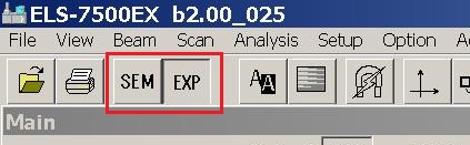
- All functions that work in SEM mode are also available and work in EXP mode.
- It is not any problem to do SEM imaging in EXP mode. However, in EXP mode, the exposure dialog is displayed and stage control is more precise by getting rid of the backlash of stage X and Y axis screws. This takes more time when moving the stage. So many operators prefer SEM mode when doing SEM imaging.