1 Build up the model layers
2 Normal Fit
3 Point-by-point fitting
4 General Oscillator Model Fitting
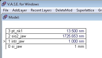
1. AddLayer "si_jaw.mat" as the substrate in the Model window.
2. AddLayer "Intr_jaw.mat" as the interface between Si and SiO2 in the Model window. Check a fit box of thickness.
3. AddLayer "sio2_jaw.mat" as the tabulated SiO2 layer in the Model window. Check a fit box of thickness.
4. AddLayer "pt_nk1.mat" as the tabulated Pt layer in the Model window. Check a fit box of thickness.
5. Adjust the thicknesses of SiO2 and Pt layers close to the graph curves (in this case, ~1700 nm for SiO2 layer and ~10 nm for Pt layer).
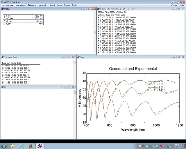
1. Do Normal fit in the Fit window, to fit the thicknesses only.
2. The MSE is 38.08.
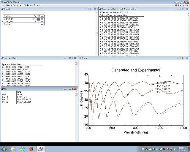
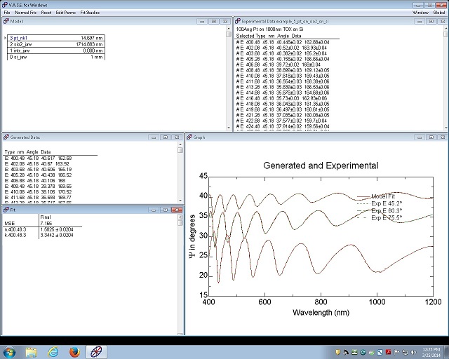
1. Check off the fit boxes of the thicknesses in all of the model layers.
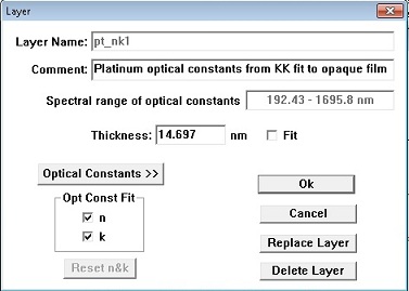
2. Check the fit boxes of n and k in the Pt model layer. Click "OK".
3. Do point-by-point fitting in the Fit window.
4. The MSE is improved to to be 7.166.
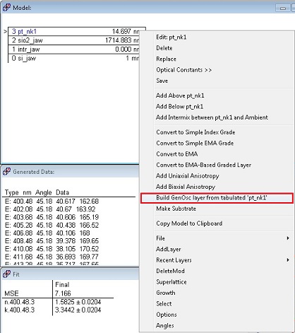
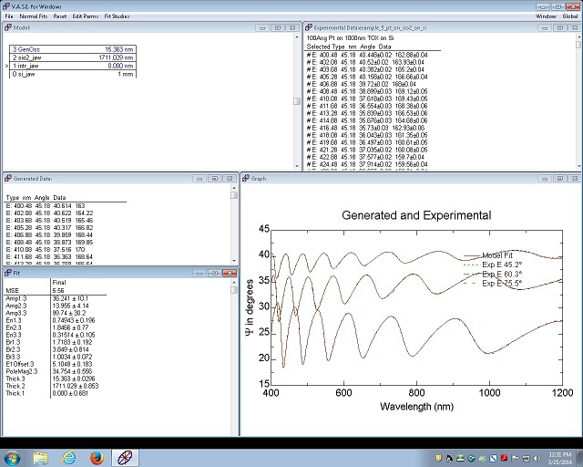
1. Convert the Pt layer to General Oscillator model layer.
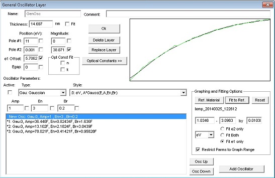
2. Fit e2 first, and then fit e1 in the GenOsc layer window. Click "OK".
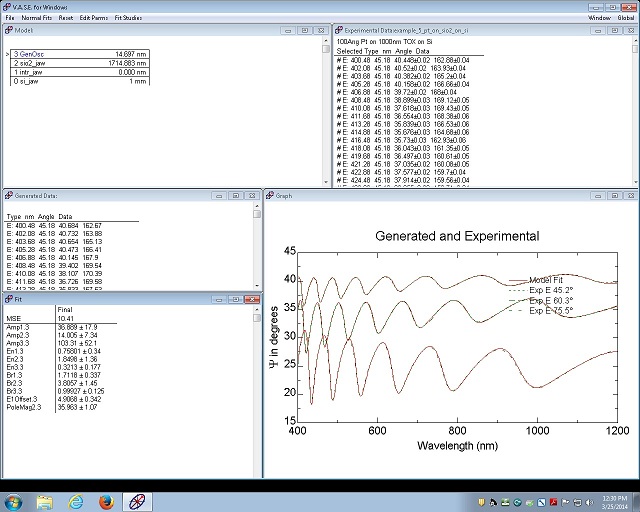
3. Do Normal fit in the Fit window.
4. The MSE is 10.41.
5. Check the fit boxes of the thicknesses in all of the model layers.
6. Do Normal fit in the Fit window.
7. The MSE is improved to be 5.56.