1 Point-by-Point Fitting
1.1 Si_jaw and cauchy.mat
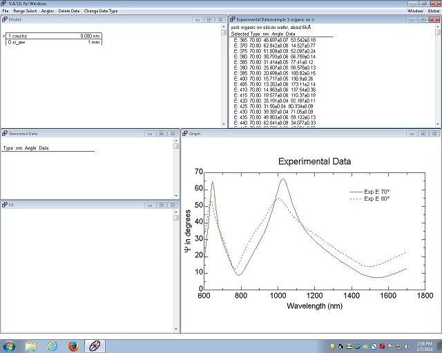
1.2 Change the spectral range to the transparent region
1.3 Fitting the raw data in the transparent region with calculation
1.4 Change the spectral range back to the whole region
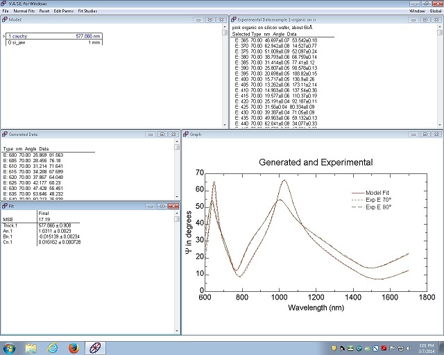
1.5 Fitting
2 Global Fitting
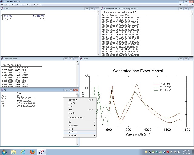
1. Repeat the Si_jaw and cauchy.mat processes in the previous section of the transparent film on Si.
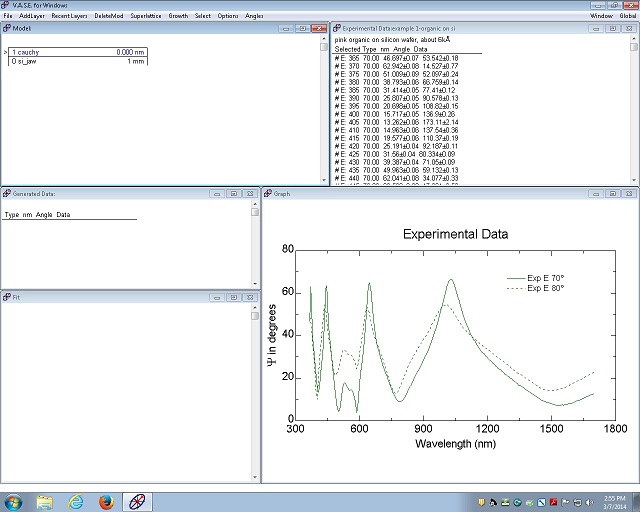
2. As can be seen in the Graph window, the interference peak heights are not the same, suggesting the optical absorption.
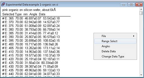
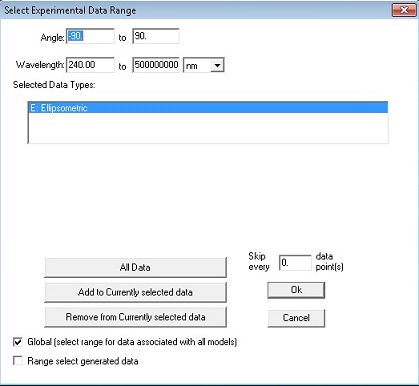
1. Right-click on the "Experimental Data" window to popup the menu.
2. Choose the "Range Select".
3. The "Select Experimental Data Range" window appears.
4. Change the wavelength range to the transparent region, and click "OK".
5. The spectral range of the graph is changed.
1. Repeat the "Adjust the thickness manually" and "Normal Fit" processes in the previous section of the transparent film on Si.
1. Right-click on the "Experimental Data" window to popup the menu.
2. Choose the "Range Select".
3. The "Select Experimental Data Range" window appears.
4. Change the wavelength range to the original region, and click "OK".
5. The spectral range of the graph is changed.
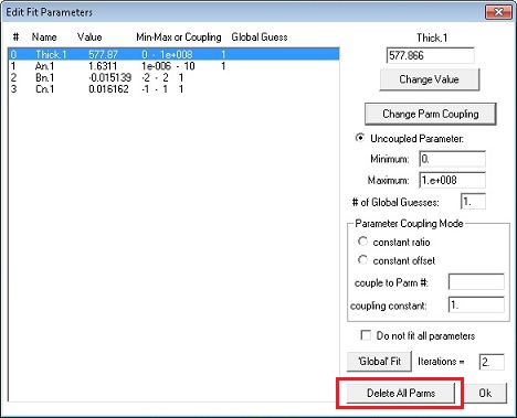
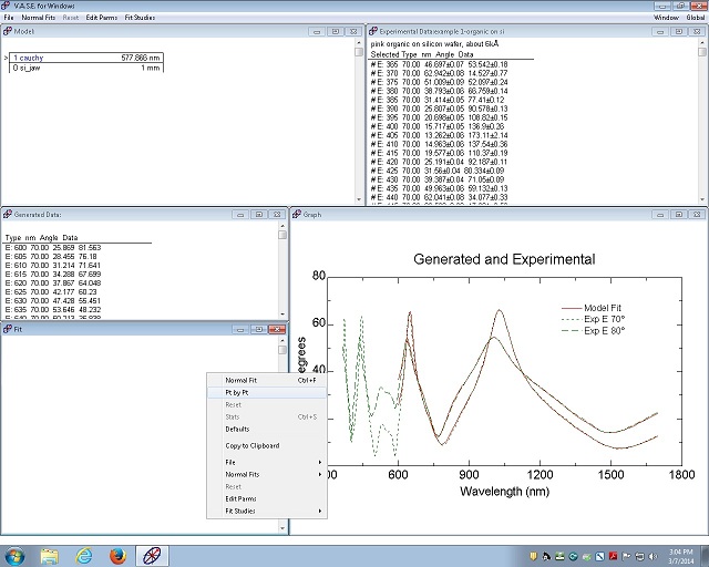
1. Click on the "Fit" window to popup the menu.
2. Choose "Edit Parms".
3. The "Edit Fit Parameters" window appears.
4. Click "Delete All Parms" to check off Thickness, An, Bn, and Cn in the Cauchy model window.
5. Click "OK".
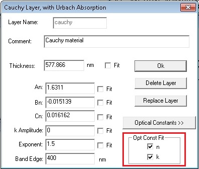
6. Open the Cauchy model window.
7. Check n and k in the "Opt Const Fit" box.
8. Click "OK".
9. Right-click on the "Fit" window to popup the menu.
10. Choose "Pt by Pt".
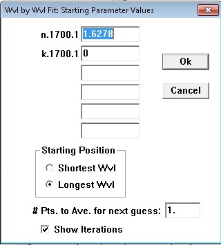
11. The following dialog box appears.
12. Click "OK".
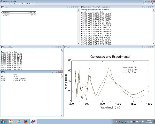
13. The fitting result is shown in the "Fit" window.

