
1 Si_jaw.mat
2 Cauchy.mat
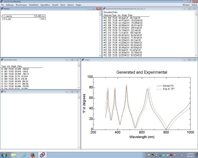
3 Adjust the thickness manually
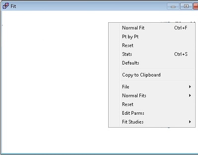
4 Normal Fit
1. Click on the "Model" window, and you see the menu change.
2. Click the "AddLayer" from the menu or the drop-down menu popped up by right-clicking on the window.
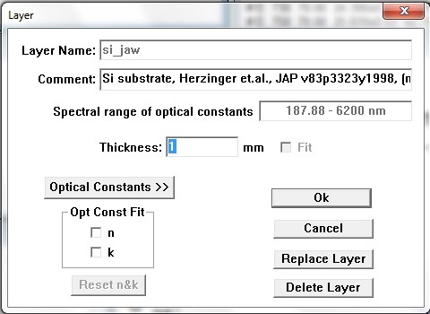
3. Choose "Si_jaw.mat" from the file directory, as the Si substrate.
4. The "Layer" dialog box appears. Click "OK".
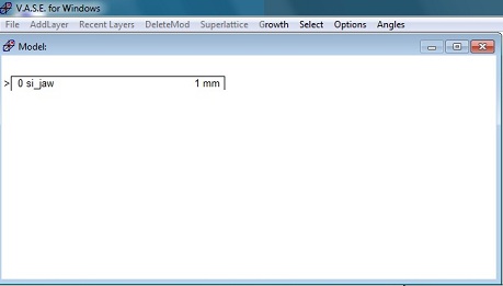
5. The Si substrate is shown in the "Model" window.
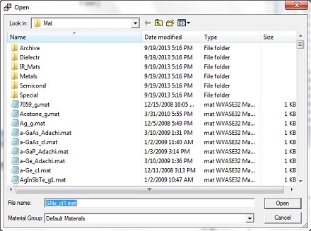
1. Click the "AddLayer" again from the menu or the drop-down menu popped up by right-clicking on the window.
2. Open cauchy.mat, which is a model for transparent or semi-transparent film.
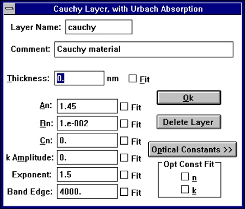
3. Cauchy Layer window appears.
4. Make sure that k amplitude is zero, because no absorption is assumed.
5. Check fit boxes of "Thickness", "An", and "Bn", and click "OK".
1. Adjust the thickness to fit the model curve with the experimental data, using a mouse.
1. Right-click on the "Fit" window to pop-up the menu.
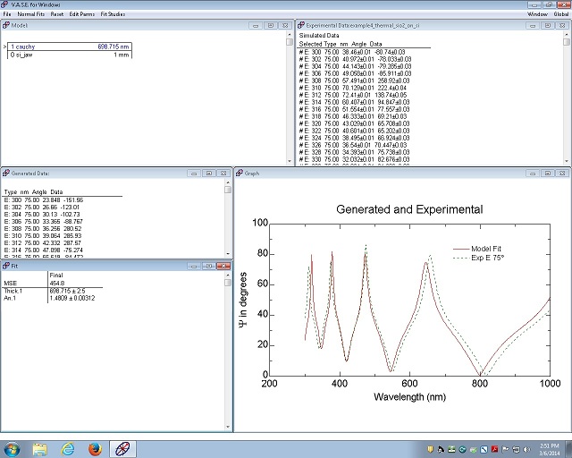
2. Click the "Normal Fit" for Thickness and An.
3. As can be seen in the "Fit" window, the thickness is 698.715 nm, and MSE (Mean Squared Error) is 454.8. The number of MSE should be less than 10 for the best fitting.
4. Open the Cauchy model window by clicking the cauchy model in the Model window.
5. Check fit box of "Bn", and click "OK".
6. Right-click on the Fit window to pop-up the menu.
7. Click the "Normal Fit" for Thickness, An, and Bn.
8. The fitting thickness is 749.865 nm, and MSE is 7.293.
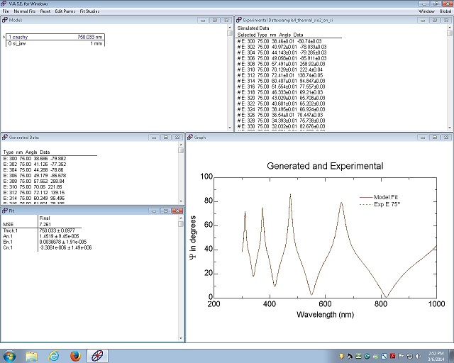
9. Open the Cauchy model window by clicking the cauchy model in the Model window.
10. Check fit box of "Cn", and click "OK".
11. Right-click on the Fit window to pop-up the menu.
12. Click the "Normal Fit" for Thickness, An, Bn, and Cn.
13. The fitting thickness is 750.003 nm, and MSE is 7.261.
14. If you want to have the better result, try to add a layer of "srough.mat", which is surface roughness correction.

