
Slide 2: The first slide was a discussion point for the different elements and what needs to be configured in order to program the device.
Administrivia: The Course Calendar is online, and contains items including handouts, slides, lecture notes (like these), reading lists and supplemental reading, and other important information. It will be continually updated during the course of the class.
Today's topics: Computing requirements for reconfigurable devices and VLSI scaling. These notes generally follow the slides, and the numbers refer to the order in the handed out slides.
Slide 2: The first slide was a discussion point for the
different elements and what needs to be configured in order to program
the device.

Slide 3: These are two sample programmable devices, a large
block of memory or combinational logic. The problems are potential
inefficiencies, the exponential size in the memory, feedback and
routing issues, and, most importantly, NO STATE! This slide was
designed as a discussion point. Without state, there are limits on
reuse of components, and, if an infinite input stream is required, the
lack of state implies an infinite number of these devices are
required.

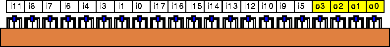
Slide 4: We need registers for pipelining (for performance),
to communicate data between cycles (eg in an FSM or some feedback
loop). The general buzzword used for both these uses is
Retiming. The two pictures are two alternate data flows for an
ASCII character (0-9,a-f) to hex converter. The circles are the
inputs, while the boxes are 4 input lookup tables (4-LUTs). The first
can be pipelined by adding registers on the input, but can't be
pipelined more aggressively, because some of the inputs go to the
second row of the computation.
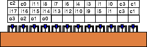
The second diagram shows the additional blocks that are used to
retime data, allowing this aggressive pipelining. Such pipelining doesn't
help latency, but will help bandwidth.
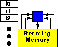
Shown below is a simple model for our configurable computing device:
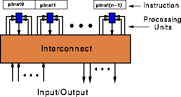
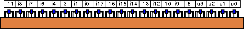
Mapping the ASCII hex->binary circuit onto such a device, we program up the instruction to evaluate each of the constituent compute blocks and configure the interconnect accordingly. Shown below is the device programmed up without the additional retiming blocks.

Slide 5: So why don't we always just fully pipeline and run
at the maximum speed? Sometimes there is feedback, where the final
output is needed as an input to the next calculation (forcing
serialization), or perhaps the application doesn't require as much
throughput.
If either of these is the case for our ASCII hex->binary example, evaluation would proceed as follows (active instructions highlighted in yellow):
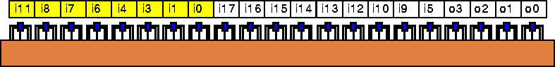
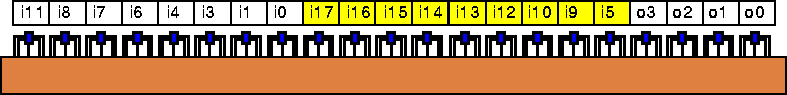
Most of the circuitry is left idle at any point in time.
In such cases, we may use less hardware, possibly without affecting the latency (but at a definite cost of throughput). For example, the 3 separate rows of operations in the ASCII hex->binary example could be implemented with a single block of 12 computational units by first doing the actions of the first row, then the second, then the third. In order to do this, we need to be able to quickly change the array's behavior, essentially having multiple instruction.
We also need to be careful that all data is in the right place. A few extra blocks are allocated here --- just as in the fully pipelined version --- to retime data so that the correct version of each value is available to each compute block when it is evaluated.
An even smaller implementation is possible with more storage and instructions but a single lookup table. Since data and instruction storage is usually much smaller, this takes less area but impacts performance.
Another way of putting it is that the data flow graph may allow full pipelining, but that the application either (a) might not require the full throughput or (b) might contain a feedback loop which prevents pipelining. Nonetheless, we can still use the techniques involved in pipelining to instead make the problem more area efficient. Instead of having hardware to compute the entire calculation, we can have sufficient hardware to perform only 1 of the pipeline stages, store the result, reconfigure the hardware to perform the next stage, store the result etc. This requires that we store multiple configurations (essentially a few VVLIW (Very Very Long Instruction Word. :) instructions which we can quickly switch between. Due to the extreme size of these instructions, we can't expect to load these from external memory)

Slide 6: Sometime there are mutually exclusive cases (EG,
if else constructs). We can share hardware by doing one or the other,
which we can do by either changing/selecting the instruction based on
the data (like a conditional branch in a conventional computer), or by
building a device that does one or the other (eg ALU) with the mode
selected by the data. One example might be an FSM, where the states
CHANGE the operation of the logic, allowing a much more complex FSM to
be built in the same amount of hardware.

Slide 7: This is the extreme example of just a single
computing element, which is very area efficient but with really low
throughput. This is essentially a conventional computer with a very
small reconfigurable functional unit and a register file. As such,
the calculation needs to be performed sequentially, so the throughput
decreases linearly with the number of gates required.

Slide 8: Wrapup slides for this discussion: We need both
computing elements and interconnect. The application will give us the
throughput, which we can use to make things more efficient by reusing
element on different data (pipelining for throughput) or by reusing
the same elements for different parts of the computation (sacrificing
throughput for area).

Slide 9: Reuse means we must have some way of data
retiming, and often an ability to change instructions. Memory itself
can be used for data retiming or for holding the inactive (but soon to
be used) instructions. This memory may often be scattered throughout
a reconfigurable device or may be as one or two monolithic pieces.

Slide 10: (Note, the lecture occurred in a different order,
with this shifted to the end. These notes follow the slides
however). FPGA marketeers' speak in terms of gate counts, but they
aren't the only thing (have interconnect and state elements) and the
notion of counting gates is tricky.


Slide 11-12: How many 2-input NAND gates are in a 2 input
lookup table (2-LUT)? Depends on what kind of gate! So really a
range.(1-4). Xilinx generally takes something of a midpoint when they
give the numbers (eg, a XC4000 4-LUT would be (1-9) or so, so Xilinx
says 4 or 5) (How Xilinx counts gates).

Slide 13: And then what about a flip-flop? It's probably 6
or so IF you use it, but if you don't, well?

Slide 14: Interconnect makes it more difficult. EG, the
left one is more area efficient (the right one has a full crossbar,
which grows with the square of the number of gates), but the yield may
depend on application, eg, the routing on the left one is VERY bad,
and may really hurt yield, while the one on the right will be able to
use all the gates. But for some applications, the limited routing
available on the left is sufficient.

Slide 15: Needed retiming also affects things. How many ffs
to retime the 1st example? Well, 22 gates? But on something like the
XC6200 (a FF/LUT structure), you need 4 blocks, so 40? gate
equivalents? What happens if the LUT can be used for memory?

Slide 16: Conclusion: Why should we count one element when
all three (compute, retiming, interconnect) are all important. Any
architecture has a fixed ratio (but some items may be used for 2 or 3
functions), so measuring a single item is misleading unless it is the
limiting factor for a specific application.

Slide 18: Scaling VLSI. We need to predict what the
technology of the future will be in order to model/reason about
current trends and devices to be built later.

Slide 19: Scale everything uniformly, either by a factor or
by measuring something that is scaled (lambda). Dennard postulated
that this would be good down to 1 micron (it was), and Bohr has
shown that we've managed to continue this. The scaling concept
appears to be valid at least for another 10 years.

Slide 20: Shows how we scale different features, which has been
true for all but voltage. Voltage over the long term follows the
historical trend, but it tends to stay at one level for a considerable
time before moving to a lower value, mostly for compatibility reasons.
(EG, 5 volts remained the standard voltage for a considerable time)

Slide 21: Shows area comparison. 1st is die size for
various devices, the second is their area in lambda^2, and the third is
relative area in terms of lambda^2.


Slides 22-29: Math for scaling all the other quantities. Note
that wire delays DO NOT SCALE, and actually get worse as wires get
longer (in terms of lambda) to get across chip. There are also two
ways to calculate energy dissipation. The resistive model is
appropriate for NMOS (or non-complementary structures in CMOS such as
grounded-P gates), and suggests that power per gate goes
down by the square of the scaling, which implies that if the scaled
process has more transistors/unit area by the scaling that the power
per unit area will remain constant. The capacitive dissipation model
is more appropriate for CMOS, where most of the dissipation is the
charging and uncharging of the capacitors.

Slide 30: Summarizes all the scaling.

Slide 31: Notes: Circuit delay does not scale as fast,
because of wire delays. Adding wire layers, and thicker wires help
some, but not enough.