Updated on 5/27/2015
1 Process Flow
2 Resist Film Coating
2.1 Preparation
2.2 Assessment
3 Exposure
3.1 General
3.2 Mask Alignment and Assessment
4 Developing
4.1 General
4.2 Assessment
5 Etching a underlying layer
5.1 General
5.2 Assessment
6 Depositing an additional layer
6.1 General
6.2 Assessment
7 Resist Stripping
7.1 General
7.2 Assessment
8 Inkjet Printing---Maskless Patterning
This section introduces basic nano- and micro-fabrication concept. Nano- and micro-fabrication can be done by the following consecutive processes:
1. Resist film coating on the substrate
2. UV, e-beam, or laser exposure of the resist film
3. Develop the resist film in a developing solution
4. Etch an underlying layer or deposit an additional layer through the developed resist film
5. Strip the resist film in a stripping solution
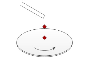
The resist film is normally spin-cast onto the substrate, and the thickness depends on the resist (PMMA, 100-300 nm; S1800 series, 1-5 μm; SU-8, ~50 μm). Figure 1 shows a relationship between spin speed and film thickness of S1800 series positive photoresist. As can be seen in Fig. 1, the film thickness decreases with increasing spin speed. Users can choose the type of resist and spin speed, so that the desired film thickness is achieved. The substrate should be ultrasonicated with acetone and alcohol (methanol or isopropyl alcohol), and dried with nitrogen before the spin cast. The resist solution should be filtered one or two times when it is taken from the original bottle. A filter-syringe is commercially available. The filter-syringe should be washed with solvent before use, in order to remove any contamination present on the filter.
Next, the film is baked on a hot plate or in an oven to remove the solvent from the film before exposure. Please see the detail of the desired resist film in Resists and their supplements.
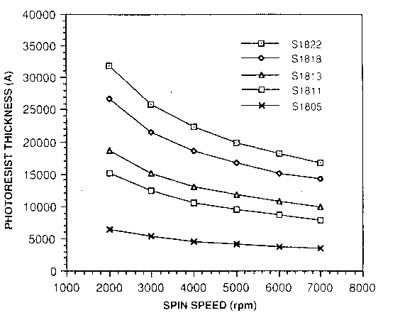
Figure 1. Relationship between spin speed and film thickness of S1800 series
The film thickness is measured using a stylus profiler and/or ellipsometer. If the substrate is not cleaned, or if some small particles are contained in resist solution, spot-like interference fringes and/or streaks are observed on the film.
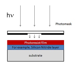
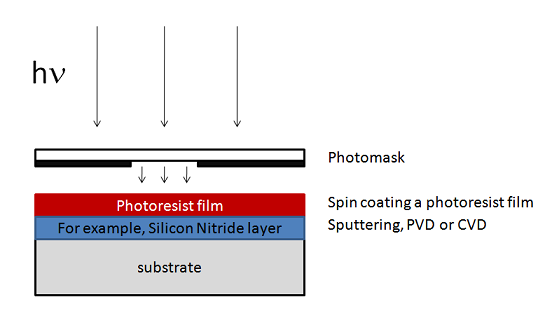
Figure 2 shows exposure onto the photoresist film through a photomask; the desired area of the film is exposed through the transparent areas of the photomask. The substrate of photomask is soda lime, boron silicate, or quartz, depending on transmission of the UV light. The masking material is chromium. The mercury discharge lamp's g-line (436 nm), h-line (405 nm), or i-line (365 nm) is used in most cases, but deeper UV light is also available. The limit of resolution is ~1 μm for contact photolithography, depending on the tool and worker's skill. Some resist films are required to be postbaked after exposure.
Figure 2. Exposure of a photoresist film
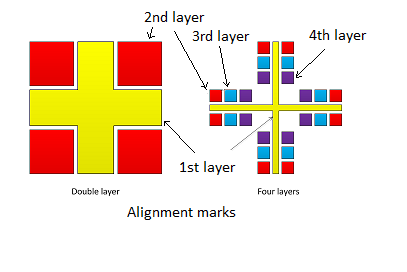
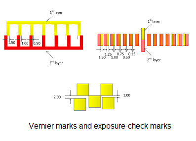
Mask alignment is required when multi-layer structures are fabricated, so that the multiple-layers correctly overlap. Alignment marks are placed onto the photomask in addition to the device patterns. Furthermore, vernier marks can also be included to quantify of the alignment. Figure 3 shows alignment and vernier marks overlapping between succesive layers.
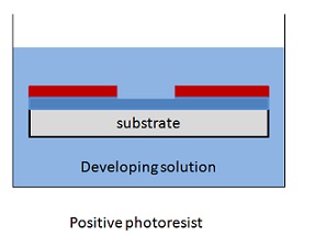
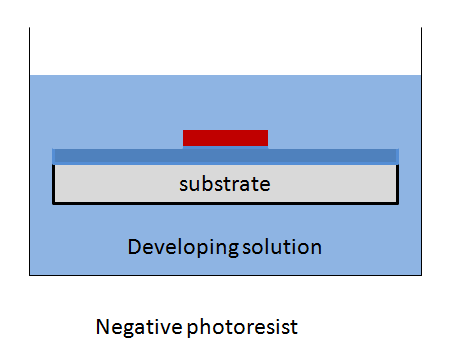
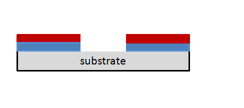
Figure 3. Alignment and vernier marks overlapping between successive layersThe exposed resist film is developed in an alkaline solution, which is commercially available, e.g. MF-319 and CD-26. The photo exposure changes the chemical structure of resist, so that dissolvability of the positive resist film is increased by the exposure, whereas that of the negative resist film is decreased. Figure 4 shows developing of the positive and negative photoresist films. As shown in Fig. 4, the exposed area in the positive film is dissolved by the developing solution, while the unexposed area in the negative film is dissolved.
The developed resist film is assessed by an optical microscope, scanning electron microscope (SEM), and/or atomic force microscopy (AFM). When the size of the structure is in a micron order, the optical microscope is commonly used to assess the film. If the size is submicron, then SEM or AFM is used.
The underlying layer can be etched through the developed resist film by a wet or dry method. Figure 5 depicts a cross section of an etched underlying layer through the developed resist film. In the wet method, the sample is immersed in an acidic solution, so that the solution etches the underlying layer through the developed area. In the dry method, energetic reactive ions from plasma are used to bombard the exposed layer. Typical gases used in reactive ion etching (RIE) are carbon tetrafluoride (CF4), trifluoromethane (CHF3), sulfur hexafluoride (SF6), chlorine (Cl2), boron trichloride (BCl3), and oxygen (O2). CF4, CHF3, and SF6 are used to etch silicon, silicon nitride, and silicon oxide, but not metals. Cl2 and BCl3 are used to etch aluminum and gallium arsenide (GaAs). On the other hand, other materials, e.g. aluminum nitride and aluminum oxide, are also etched by Cl2 and BCl3 plasma in Penn Nanofab. Oxygen plasma is used to remove organic materials, e.g. resist residue.
Figure 5. Eching a underlying layer through the photoresist film
The cross section of the etched underlying layer is examined with SEM and/or AFM after stripping the resist film. When SEM is used, the cross section is prepared by cleaving the sample, or by making a micron-size trench on the sample using focused ion beam (FIB). When AFM is used, the cross section is directly observed with a cantilever tip, without preparation of the cross section.
A possible problem is lateral-etching. Since the wet etching is isotropic, care should be taken with the etchant solution concentration, etching time, and temperature. On the other hand, the dry etching is anisotropic because energetic ions are directed towards the sample surface. However, the lateral-etching is also observed (although to a lesser extent) because of reactive ions travelling parallel to the sample surface. This problem can be minimized by optimization of plasma parameters, i.e. gas pressure, flow rate, bias voltage, temperature, and the etch chamber geometry.
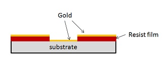
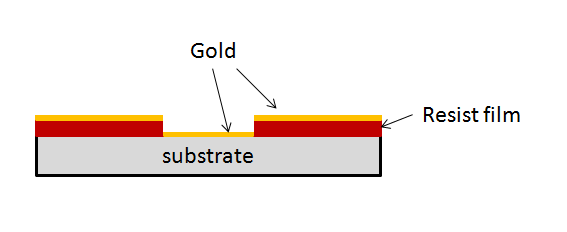
An additional layer, which is usually metallic, is deposited onto the developed resist film. Figure 6 shows deposition of a gold film onto the developed resist film. As can be seen in Fig. 6, the gold film is deposited on both of the resist film and the substrate. Deposition can usually be done using thermal evaporation, e-beam evaporation, DC and/or RF sputtering. Chemical vapor deposition (CVD) is not used in this process, because the high temperature of the substrate during CVD process melts or burns the resist film.
Figure 6. Deposition of a gold film on the developed resist film
The sample is assessed by an optical microscope, SEM, and/or AFM after stripping the resist film. Possible problems are described in the next section.
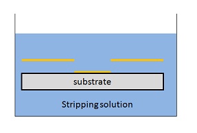
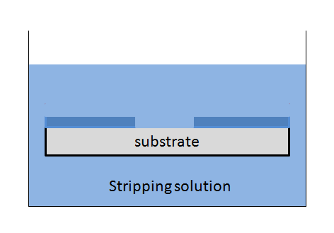
Figure 7 shows stripping the resist film by immersing the sample in a stripping solution, which is acetone or commercial stripping solution, e.g. Remover PG. These stripping solutions are available in Penn Nanofab.
Figure 7. Stripping the resist film after the etching process
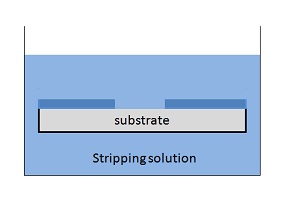
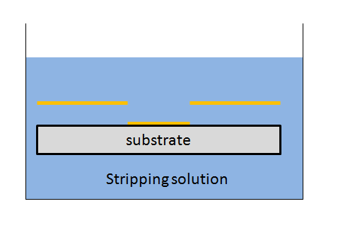
Figure 8 depicts lift-off of the gold film in the stripping solution; when the sample is immersed in the stripping solution, the resist film under the gold film is dissolved away, so that the gold film is lifted off. On the other hand, the gold film deposited on the substrate is not removed.
Figure 8. Lift-off the gold film.
A possible problem after the dry etching process is that the resist film cannot be removed completely with the stripping solution. This can happen when the resist film is exposed to plasmas for a long time, due to increase in the temperature of the sample, or changes in the chemical structure of the resist film. The resist residue can normally be cleaned by oxygen plasma. However, it is sometimes very difficult to remove it because some portion of the resist residue is carbonized in the worst case. To avoid this problem, the dry etching process should be divided into several steps. For example, if ten minute etching time is required, it is a good idea to repeat a process of 1 minute etching and 30 second off, to cool down the film.
Sometimes the deposited film on the resist film does not lift-off. This happens when:
(1) The lift-off layer is too thick; a simple rule of thumb for thickness of the lift-off layer is less than one third of that of the resist film.
(2) The resist layer has not been properly prepared for lift-off, i.e. a positive slope allows the lift-off material to form a continuous film across the sample even though the thickness ratio has been properly selected. This problem can be solved by using the bi-layer method (with the aid of LOR or PMGI) or by image reversal. Check the detail of LOR 3A and/or PMGI in Resists and their supplement.
(3) The resist film is burned or melted by the high temperature of the lift-off layer substrate when the lift-off layer is deposited in the vacuum chamber.
This is a micro-printing technology of non-contact and maskless patterning of the thin film device on rigid and/or flexible substrate. Furthermore, a device design can be changed anytime on the computer. The "ink" is prepared by dissolving or dispersing the specimen in volatile solvent, and is stored in a cartridge. Then, the thin film device is jet-sprayed on the substrate, like in normal printing. Please refer to the detail of the following review article. Inkjet_Printing-Process_and_its_Applications; A resolution of 20-40 μm has been reported. The following devices have been reported using inkjet printing: organic thin film transistor, light emitting diode, solar cell, magnetic memory, gas sensor, biological, and pharmaceutical devices.

