|
The silicon (and to a lesser extent, silicon alloy) crystal growth and wafer processing industry continues to generate a large experimental database characterizing the properties of numerous defects and impurities that plague microelectronic devices. This extensive database is tremendously useful for multiscale model development and testing because the defects of current interest (voids, dislocation loops, impurity complexes) are nanoscale features that are spatially distributed over macroscopic length scales, i.e. in wafers and crystals. It is also notable that many of the microscopic mechanisms responsible for defect generation and evolution are generally important for understanding a broad range of phenomena. Our work in this area therefore is motivated by two complementary needs:
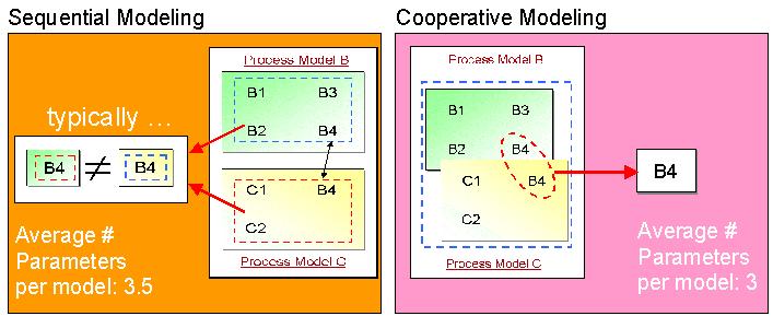
An important aspect of the experimental database is its heterogeneity, i.e. there are many different types of measurable data available from different experiments. However, many of these data (and therefore the models for predicting them) are connected at the atomic level because they are all dependent on the same basic diffusion, reaction, and aggregation of simple point defects such as vacancies, interstitials, and impurities that are always present. Despite the decades of research in this area, a major obstacle in the development of robust and predictive process models for the silicon crystal growth industry has been, and continues to be, the uncertainty associated with the thermophysical properties of these building blocks. Our contributions in this area include the development of a comprehensive suite of continuum models for various phenomena including point defect dynamics during crystal growth, void formation, metal diffusion in wafers, and oxide precipitate formation. However, rather than consider each of these models and their associated parameters separately, we have developed an inverse modeling framework that allows for the simultaneous consideration of multiple phenomena thereby taking advantage of the common microprocesses. As shown below, this approach has two advantages over the traditional sequential one: (a) the number of regression parameters is reduced, and (b) the robustness of the parameters is increased because only a single value for each one is allowed.
Figure 1: Cooperative approach for multiple-model regression leads to fewer effective parameters and greater exposure to experimental data.
|
![]()