
6.3. Homework Submission
Your writeup should follow the writeup guidelines. Your writeup should include your answers to the questions below. Even if a certain question(like 1-(c) or 1-(f)) is just a “step”, please include it in your report and leave the bullet blank for the sake of easy grading.
Accelerator Interface
Run CPU version on Ultra96, and report the latency.
For FPGA version, copy in the
xrt.inifile into the Ultra96 and run the code. Copy the Vitis Analyzer files to your computer and open it with Vitis Analyzer. Click Profile Summary, and then Summary to see Total application runtime and Total kernel runtime. Click Kernels & Compute Units to see only the kernel execution time. We will check these three latencies throughout this HW. Report the latencies.In the previous step, you must have seen warnings regarding unaligned host pointer. You will now allocate contiguous host memories. Take a look at Step 2 in this tutorial. In
apps/mmult/fpga/HostAligned.cpp, we kindly provide three TODOs for this step.Hint
As shown in the example link, you should only use the following flags when allocating memory using cl::Buffer: CL_MEM_READ_ONLY, CL_MEM_WRITE_ONLY, CL_MEM_READ_ONLY | CL_MEM_WRITE_ONLY. All other flag usage prevents contiguous memory allocation or behaves non-deterministically on the Ultra96 (i.e. when using CL_MEM_USE_HOST_PTR).
Build the project with the modified host code. Because only the host code is modified, it should take less than a minute to complete. Copy only neccessary files and report the three latencies in the Vitis Analyzer.
In the Vitis Analyzer, open the application timeline. Zoom in at the beginning of the kernel execution, and provide a screenshot in the write up. Based on the analyzer, suggest at least two ways of improving the performance of the FPGA code.
We will now modify the kernel code.
In terminal, make sure you correctly sourced the settings, and open Vitis HLS, with:
vitis_hlsClick on open project and browse to the your build generated directory:
hw6_fpga_kernels/Hardware/build/mmult_fpga/mmult_fpga/mmult_fpgaand click open.
Partition the HLS code into Load-Compute-Store Pattern as can be seen in this code and this tutorial. Enable dataflow with
HLS DATAFLOWpragma and usehls::streamto pass data between Load, Compute, Store functions. Make additional changes to the code to achieve II=1.Make sure to run C simulation and verify that your HLS code is functionally correct. Provide the code in your report. Also, provide the screenshot of Performance & Resource Estimates table in the Synthesis Summary Report. Because you have Load, Compute, Store functions, expand each function in the table to show that you achived II=1.
Rebuild the project with the dataflow-enabled kernel, copy the binaries and boot files, reboot and test. This will take about 30 minutes to build. Report the latencies. Provide a screenshot of the relevant section of Application Trace from Vitis Analyzer.
Our initial FPGA host code uses an in-order command queue. Find out how to use an out-of-order command queue to get overlap between communication and computation. Make the necessary change in the
Host.cppand provide the change in the report. Build the project with the modified host code. Report the three latencies. Provide a screenshot from Vitis Analyzer. We expect you to see something like Fig. 6.3 or Fig. 6.4.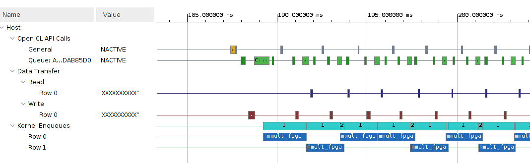
Fig. 6.3 Communication and Computation overlap
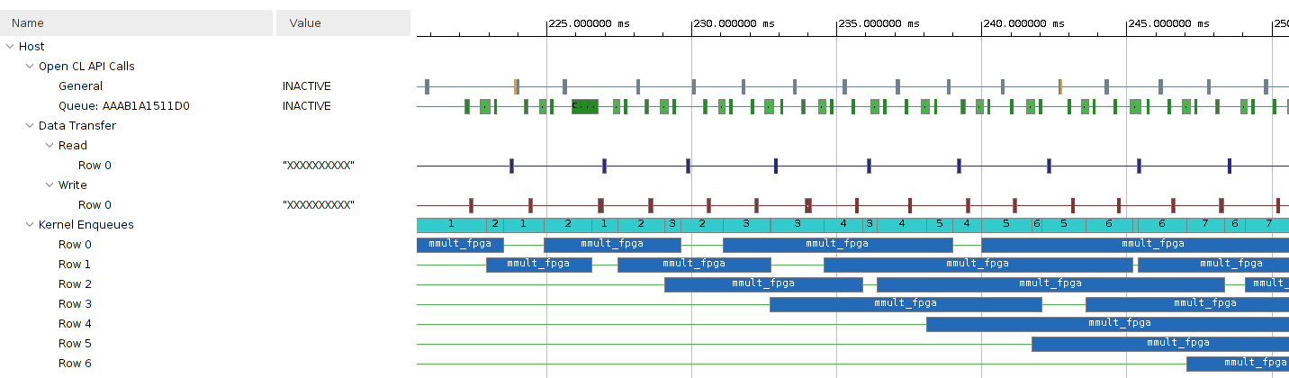
Fig. 6.4 Communication and Computation overlap when a kernel runtime is longer
Use the following command in your host machine. Report the clocks, memory ports and resources that are available on the platform:
platforminfo $PLATFORM_REPO_PATHS/u96v2_sbc_base.xpfm
Read about kernel and host code synchronization from here. Add a barrier synchronization for every 8 tasks to your host code. Build the project with the modified host code. Run it and provide a screenshot of the relevant section of vitis analyzer.
Assign separate ports to the
mmult_fpga. In the Assistant view on the lower left corner, hw6_fpga_system_hw_link\(\rightarrow\)Hardware\(\rightarrow\)binary_container_1. Open Binary Container Settings, and in Compute Unit Settings, you can assign the ports. This will take about 30 minutes to build. Report the latencies. Provide a screenshot of the relevant section of Application Trace from Vitis Analyzer. Does assigning multiple ports on Ultra96 have any impact on your design? Save/Move thehw6_fpga_system_hw_link/Hardware/binary_container_1.buildfolder of the project to somewhere else before doing the next question. We will use the outputs from this question in the next part.Learn about how to use multiple compute units from here and apply it to your design. Use 2
mmult_fpgaunits. This can also be done in the Compute Unit Settings we visited in the previous question.
Rebuild the FPGA version, copy the binaries and boot files, reboot and test. This will take about 30 minutes to build. Report the latencies. Provide a screenshot of the relevant section of Application Trace from Vitis Analyzer. If you are run out of the FPGA resources, report it.
Analyze Implementation
In this question, we will investigate what the FPGA implementation of the matrix multiplication (1m) look like using Vivado (not Vivado HLS). Vivado is part of the Vitis installation.
Report how many resources and utilization percentage of each type (BlockRAM, DSP unit, flip-flop, and LUT) the implementation (1-(m)) consumes. You can find this information in the Implementation tab on the left hand side. Click Report Utilization under Open Implemented Design. Launch Vivado using the following commands and open the project you saved/moved from the location
binary_container_1.build/link/vivado/vpl/prj/prj.xpr. (4 lines)In terminal, make sure you correctly sourced the settings, and open Vivado, with:
vivado
Report the expected power consumption of this design by clicking Report Power of the Implementation tab. (1 line)
On the left top corner, you will see IP Integrator. Click Open Block Design under IP Integrator. Open the Address Editor by choosing the corresponding tab above the block design. In which memory region is the control interface of the accelerator wrapper
mmult_fpga_1mapped? This region is used for such communication as starting the accelerator and querying its status. Writes and reads by the ARM processor are to this region are sent over an AXI4-Lite bus to the accelerator wrapper, which handles them and controls the accelerator. (1 line)Open the timing report by going to the Implementation tab and pressing Design Timing Summary from the Timing tab. Click on the number next to Worst Negative Slack. Look at the
Path Properties. Report in which of the hardware modules that we saw in the block design the path begins and ends. (1 line)Include a screenshot of the critical path in your writeup. Zoom in to make sure all elements of the path are clearly visible. Indicate the type of each element (e.g. LUT, flip-flop, carry chain) on the screenshot.
Highlight the accelerators in green, the interconnect (
M_AXIandS_AXI) in yellow. You can do this by right- clicking the modules in the Netlist view and selecting Highlight Leaf Cells. Include a screenshot of the entire device in your report.
6.3.1. Deliverables
In summary, upload the following in their respective links in canvas:
writeup in pdf.