Updated on 6/6/2019
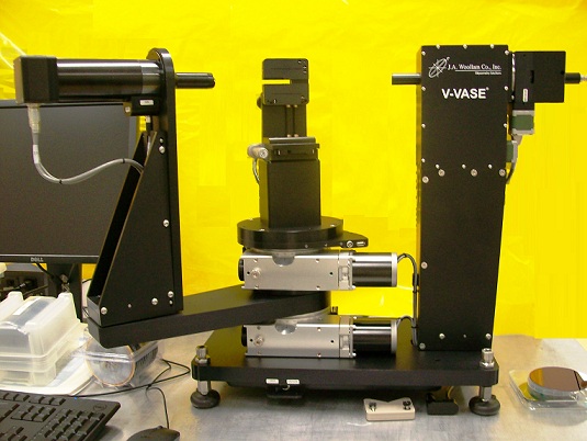
1 Cold Start
2 Initialization
3 Calibrate System
3.1 Align 25 nm SiO2 Standard Sample
3.2 Z-axis Translation Alignment
3.3 Calibration
4 Preparation for Measurement
5 Spectroscopic Scan
6 Analysis using a model fitting
6.1 Dielectric, Si, and other substrates
6.2 Cauchy model fitting for transparent film
6.2 Global fitting for thick films
6.3 Pt-by-Pt model fitting for a semi-transparent material
6.4 General Oscillator (Genosc) model fitting
7 Fitting Raw Data With Calculation
7.1 Substrate
7.1.1 Glass substrate
7.1.2 Semi-transparent substrate
7.1.3 Opaque substrate
7.2 Single layer
7.2.1 A transparent film on Si wafer
7.2.2 A partially absorbing film on Si wafer
7.2.3 A transparent or partially absorbing film on Si wafer
7.2.4 An absorbing film on glass
7.3 Multilayer
7.3.1 Multi-Layer Strategies
7.3.2 Pt/SiO2/Si wafer
7.3.3 a-Si/SiO2/Si wafer
7.3.4 TiO2/SiO2/Si wafer
7.3.5 crystalline-Si/SiO2/Si wafer
7 Advanced Fitting
7.1 Surface Roughness
7.2 Index Grading
7.3 Surface Roughness + Index Grading
7.4 Non-ideality on Data
8 Transmittance and Reflectance Measurements
8.1 Transmittance Measurement
8.2 Reflectance Measurement
9 WVASE messages on fitting
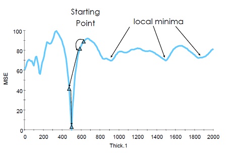
10 MSE check
11 Correlation matrix
12 Measurement on Another Sample
13 Supplement Documents
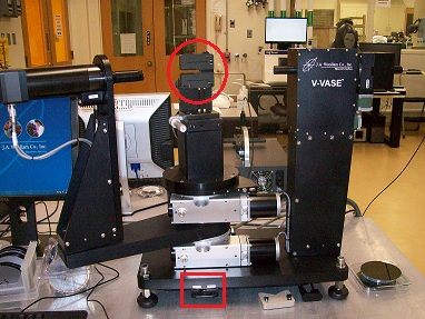
If the system is shut down, then turn on the power to the controller and monochromator (the PC is always on).
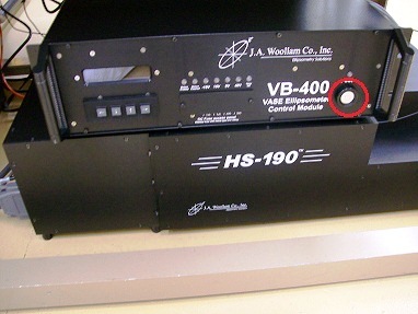
1. Turn on the control module.
2. Turn on the monochromator
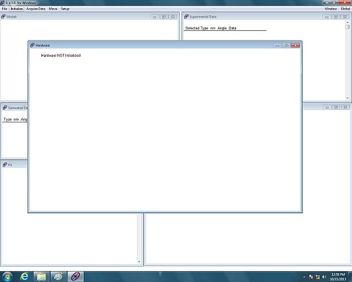
1. Double-click on the WVASE32 logo to open the software.
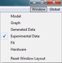
2. The following windows appear.
3. Click the "Initialize" from the "Hardware" window.
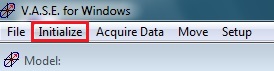
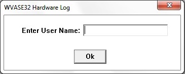
4. The following dialog box shows up. Type your name in the box, and click "OK".
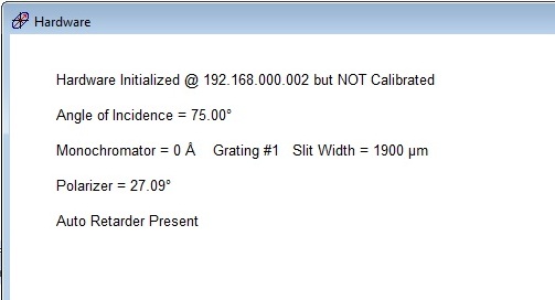
5. The following message appears in the "Hardware" window when the system is initialized.
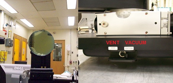
1. Load the 25 nm thick SiO2 standard sample on the vacuum chuck.
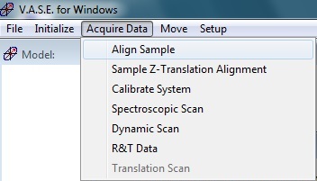
2. Choose "Align Sample" from the drop-down menu of "Acquire Data" in the menu.
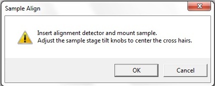
3. The following dialog box appears. Click "OK".
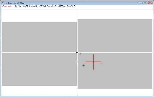
4. The sample chuck is automatically rotated to the alignment position, and the following screen is shown.
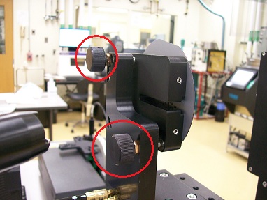
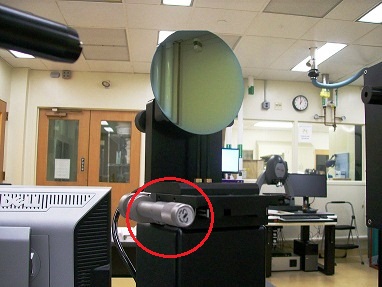
5. Adjust the red cross hairs to the center, using the two knobs behind the sample chuck.
6. Once the cross hair is aligned at the center, press the "ESC" key on the keyboard.
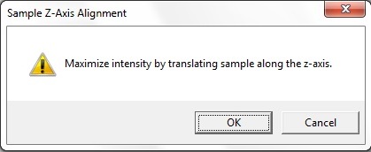
1. The following dialog box appears. Click "OK".
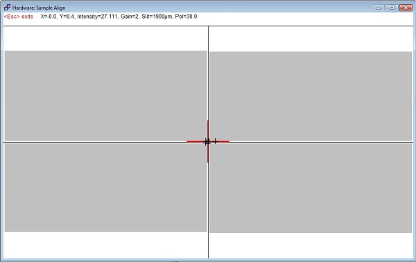
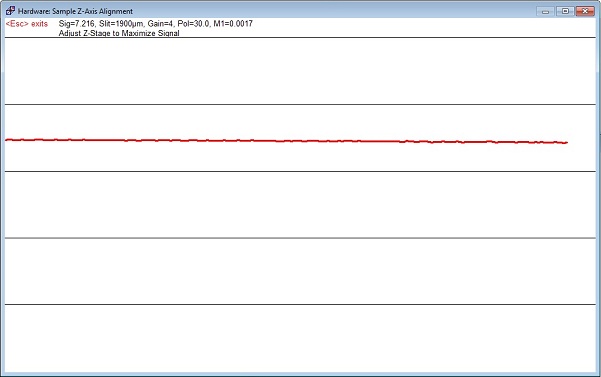
2. The sample chuck is automatically rotated to the Z-axis translation alignment position.
3. The following screen appears.
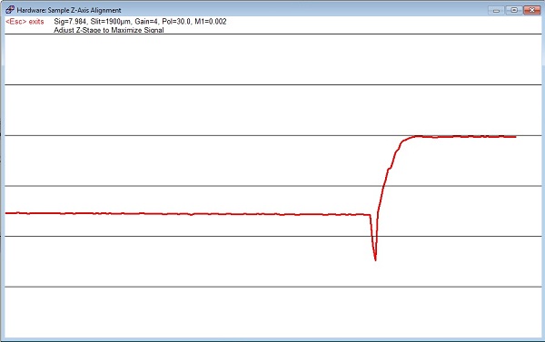
4. Adjust the intensity to be maximum, using the micrometer.
5. When maximizing the intensity, press the "ESC" key on the keyboard.
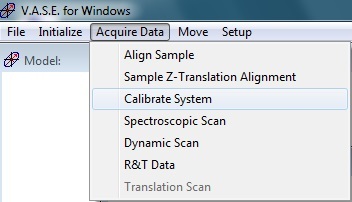
1. Choose "Calibrate System" from the drop-down menu of "Acquire Data" in the menu, which is shown on the "Hardware" window.
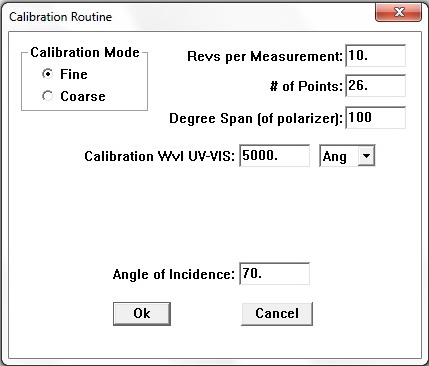
2. The following dialog box appears. Click "OK".
3. The calibration is automatically carried out.
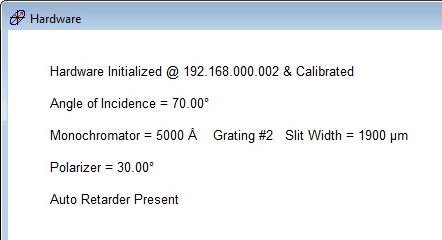
4. When the calibration is done, the following message shows up in the "Hardware" window.
1. Replace the 25 nm thick SiO2 standard sample by your sample.
2. Repeat the "Align Sample" and "Z-axis Translation Alignment" procedures shown above.
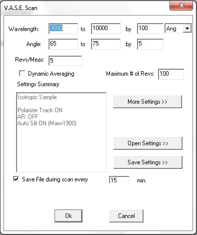
1. Choose "Spectroscopic Scan" from the drop-down menu of "Acquire Data" in the menu, which is shown on the "Hardware" window.
2. The "VASE Scan" dialog box appears.
3. Click the "Open Settings" button to load the standard scan settings.
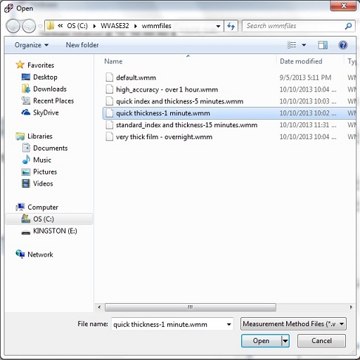
4. The following file directory appears. Choose the recipe from the file directory.
5. Enter a comment, if necessary. Click "OK".
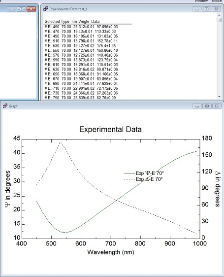
6. Spectroscopic scanning starts. The result of scanning is shown in the "Experimetal Data" and "Graph" windows.
7. Save the data, if necessary.
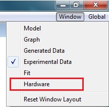
8. Close the "Hardware" window.
Genosc model fitting ensures Kramers-Kronig consistency between e1 and e2 in the analysis (see Kramers-Kronig Relation).
If you want to make a measurement on another sample, open the Hardware window, and repeat the procedure from "Preparation for measurement" shown above.


